In order to meet the ever-changing market standards and shorter time to market, programmable logic devices (PLD) are more and more widely used in circuit board and system design. The use of programmable logic devices can speed up the time to market, and has greater design flexibility compared to application-specific integrated circuits (ASIC) and application-specific standard products (ASSP). Programmable logic devices are used in many products (such as handheld devices) because of their new product architectures featuring reduced power consumption, new packaging options, and lower monolithic costs. Typical programmable logic device applications include: power-on timing, level shifting, timing control, interface bridging, I/O expansion, and discrete logic functions.
Increasingly complex system requirements have driven the demand for increased PLD logic density and increased I/O pins. Therefore, ball grid array (BGA) has become an optional packaging method for PLD. BGA packaging options, such as chip-level BGA, fine-pitch BGA, and chip array BGA, have largely replaced the quad flat package (QFP) most commonly used on most PLDs. BGA is widely welcomed by system designers, mainly because of its higher I/O density, which greatly improves the ratio of pin count to circuit board area, because it has a smaller package size than QFP package, so it is also space Ideal for restricted applications. It can save the area of ​​the circuit board and the height of the package itself. Other major advantages of BGA packages include: better heat dissipation performance, smaller misalignment tolerances, reliable package structure and proven assembly processes.
Challenges facing system designersWith the evolution of programmable logic devices, BGA packages are developing in the direction of increasing the number of pins and decreasing the pin spacing. The lead pitch or solder ball pitch refers to the distance between the centers of two adjacent pins or solder balls. The pin spacing has a significant impact on the routing of I/O from the PLD. The development trend of higher pin count and smaller pin pitch makes system designers face huge challenges, they must use more radical design rules, through advanced stacking and via technology to meet the design requirements. All in all, these factors greatly increase the cost of printed circuit boards. This article discusses some techniques that system designers can use to reduce the cost of circuit boards when designing PLDs in BGA packages.
Factors affecting the manufacturing cost of printed circuit boardsThe manufacturing cost of printed circuit boards is a major consideration for many electronic products. Various factors that affect the cost of printed circuit boards are: the number of printed circuit board layers, the choice of stacking technology and via technology, design rules and wiring skills.
Number of printed circuit board layersThe number of layers of the printed circuit board is one of the main factors affecting the cost of the printed circuit board. The term "BGA breakout" refers to the fanout and lead-out pins that are routed around the device before the printed circuit board is normally routed. BGA breakout is the most important factor affecting the number of printed circuit boards. The number of printed circuit board layers can be minimized by selecting the appropriate BGA breakout mechanism, stack model, and via technology. Most programmable logic device suppliers provide BGA breakout techniques to assist in circuit board design and layout. These techniques help to optimize the manufacture of printed circuit boards and reduce costs.
Stackup and via modelsThe choice of stack and via model has the greatest impact on reducing the number of printed circuit board layers and manufacturing costs. There are two main types of lamination technology-FR-4 lamination and high-density interconnect (HDI). FR-4 laminate technology is used for larger circuit designs, such as computer motherboards. HDI is more suitable for space-constrained applications, such as handheld devices.
Multilayer printed circuit boards use vias or plated through holes to transmit signals from one layer to another. There are four main types of vias: through holes, blind holes, buried holes (or embedded holes) and micro holes.
Through holes provide connections through the top and bottom layers of the printed circuit board. Blind vias provide a connection between the top or bottom layer and a layer inside the printed circuit board. Embedded holes or buried holes provide connections between layers inside the printed circuit board. Micro-holes are extremely small holes drilled by lasers and provide electrical connections between several layers in a multilayer circuit board. Microvias are used for HDI circuit boards.
Generally, the manufacturing cost of laminated printed circuit boards with through-holes is the lowest, and the manufacturing cost of HDI laminates with micro-holes is the highest. The manufacturing cost of laminates using blind or buried vias is higher than that of laminates using through-holes and lower than that of HDI laminates using microvias. There are several new technologies that use epoxy filling and tin film to cover the vias, which also increase the cost of the circuit board.
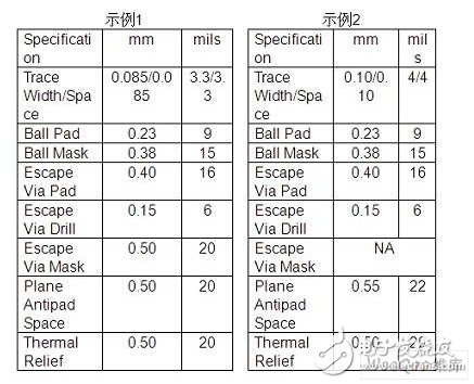
Design ruleDesign rules affect manufacturing yield and performance. When more aggressive design rules are adopted, manufacturing costs increase. Two examples of design rules are as follows. These two design rule examples use the Lattice MachXO PLD (LCMXO640-M132/MN132) in an 8x8mm, 0.5mm pitch, 132-ball csBGA package. In each example, the MachXO PLD is placed on a 4-layer laminated circuit board. Please note that Example 1 uses a more aggressive design rule of Scale 2. Therefore, the cost of the printed circuit board to meet the design rules in the first example will exceed the cost of the circuit board in the second example.

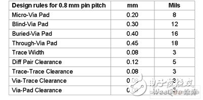
Most PLD vendors provide design rules, as shown in the table below. These design rules help reduce manufacturing costs and are supported by most printed circuit board manufacturers.
Table 1: Lattice Semiconductor's recommended SMD pads for packages with different lead pitches

Table 2: Lattice Semiconductor's recommended design rules for MachXO and ispMach4000ZE devices in 0.8mm pin pitch caBGA packages

Once the appropriate stacking technology, via model and design rules are selected, the Fanout via style becomes the most important factor that affects the number of layers of the circuit board using BGA breakout technology. The following tips can help reduce costs:
Leading out pins around the device allows more pins to be routed on the same layer. When using a BGA with a pin pitch less than 0.8mm, lead the fanout vias of the first two rows of pins to the periphery of the device and try to stay away from the BGA package. Lead them farther, so that the last two rows of pins can be led out and routed on the same layer. This will help reduce the number of printed circuit boards and manufacturing costs.
Use North, South, East, West (NSEW) or layer-based routing to improve efficiency. When only 2 to 4 layers can be used for BGA wiring, due to the extremely high wiring density, it is reasonable to lead to each layer in all directions (also called NSEW wiring). However, when the wiring that can be used for BGA exceeds 4 layers, use the layer-oriented concept, that is, the lead-out wiring conforms to the layer-oriented wiring, which can be more effective wiring.
The four-quadrant dog-bone wiring method is adopted to increase the wiring density. When leading out the pins in each direction of a layer, if the lead-out wiring and the via pattern (also called dog-bone) have different directions in different quadrants, it will help the wiring. This is an effective way to increase wiring density. The figure below shows a four-quadrant dog-bone wiring example.

Figure 1: An example of a four-quadrant dog-bone style fanout for ispMACH 4000ZE (LC4256ZE-MN144) in a 7x7mm, 0.5mm pin pitch, 144-ball csBGA package.
Please note that the four-quadrant dog-bone wiring increases the wiring channels for rows and columns at the origin of the center of the quadrant. This space can be used for more signal wiring. On the circuit board, the column and row routing channels are suitable for placing additional capacitors and pull-up resistors. The four-quadrant dog-bone wiring has lower cost and lower risk soldering problems than the via-in-pad method.
Use vias in the pads to provide space for lead-out pin routing. The use of vias in the pad can leave a space between the pad and the pad for the wiring of other signals. As the name suggests, the center of the BGA ball pad can be made into a through hole. Figure 2 shows this technique.

Figure 2: 8x8mm, 0.5mm pin pitch, 132 ball csBGA package MachXO PLD (LCMXO640-M132/MN132) uses an example of in-pad vias to lead out the pin routing.
The three rows of BGA ball pads are shown in the figure. The middle row uses vias in the pad. This technique is most useful when assembling a power plane or ground plane, because it implements a continuous power plane or ground plane under the BGA. When using vias in pads, we must remember that the backside of the circuit board under the BGA has less space for capacitors and resistors due to the routing of the pins from the fanout and vias.
Align blind holes to increase wiring density. When using blind vias, aligning the blind vias in the row and column directions is a very effective method to increase the wiring density. Particularly, it is most effective when using a BGA with multiple pin counts, and at this time, leading out the device pins is the main factor affecting the number of layers of the circuit board.
Use micro-hole HDI stacking technology to reduce the number of circuit board layers. Microporous and HDI are inextricably linked. The use of microvias is very important to reduce the number of HDI laminated circuit boards.
Summary of this articleAs the pin pitch of each generation of ball BGA packages becomes smaller and smaller, it is necessary to develop new printed circuit board manufacturing processes and signal via types to deal with higher board layout complexity. By looking at the ball packaging density and pin spacing of programmable logic devices, the application's I/O signal requirements, and the production constraints of printed circuit board manufacturing equipment, system designers can better make trade-offs between design decisions. Most programmable logic device suppliers publish printed circuit board layout tips and BGA breakout examples on their websites. System designers can use this information to reduce printed circuit board costs.
Dongguan Guancheng Precision Plastic Manufacturing Co., Ltd. , https://www.dpowergo.com