Abstract: CXA2075M is a video decoding chip produced by SONY company. This chip can convert the analog RGB signal into a combined video signal, which is very suitable for image processing conversion between personal computers and high-definition televisions and applications in electronic game consoles. The article analyzes the structure principle and main characteristics of CAX2075M, and gives the typical application circuit of CAX2075M.
1 Overview
CXA2075M is a video decoding chip produced by SONY company. It can convert analog RGB signals into combined video signals. The chip has different pulse generators, so it can meet the needs of encoding. It can encode the input composite synchronization signal, subcarrier and analog RGB signal to output the Y / C output signal of the combined video and S terminal. Compared with CXA1645M? CXA2075M has the following excellent performance?
(1) The number of external components is reduced to five, and only the components such as clamping capacitor, adjustable capacitive reactance, filter resistance, etc. can be used;
(2) There is a wave trap inside, therefore, the wave trap can not be used outside the device;
(3) The RGB output frequency band is higher than CXA1645M.
CXA2075M can be widely used in VGA interfaces of high-definition TV and digital TV, personal computer and TV video converters and electronic game conversion interface circuits.
figure 1
The CXA2075M chip uses a bipolar silicon monolithic integrated circuit process. Its main electrical parameters (maximum rating) are as follows:
â— Power supply voltage VCC: 12V;
â— Working temperature Topr: ï¼20 ~ + 75 ℃;
â— Storage temperature Tstg: ï¼65 ~ + 150 ℃;
â— Allowable power consumption PD: 780mW.
2 Pin description
The internal structure and pin arrangement of CXA2075M are shown in Figure 1. The functions of each pin are as follows:
1 foot (GND1): Ground terminal of all circuits except RGB, including the ground of video and Y / C output circuit. When wiring, the connection of GND1 should be as short and wide as possible.
Pins 2 to 4 (RIN, GIN, BIN): Analog RGB signal input.
5, 9, 11, 13, 14, 18 feet (NC): empty feet.
Pin 6 (SCIN): Sub-carrier input. Can input 0.4 ~ 5.0Vp-p sine wave or pulse.
7-pin (NPIN): NTSC and PAL system conversion end. When connected to VCC, it is NTSC, and when connected to GND, it is PAL.
figure 2
8 feet (BFOUT): BF pulse monitoring output. Can drive 75Ω load.
Pin 10 (SYCNIN): The input terminal of the composite sync signal is at the TTL level, and should be less than 0.8V when it is low; it should be high (more than 2.0V) during the SYNC.
12 feet (Vcc1): power supply of all circuits except RGB.
15 feet (COUT): Color saturation signal output terminal. It can drive 75Ω load for C signal output of S terminal.
16 feet (YOUT): Y signal output terminal. It can drive 75Ω load for Y signal output of S terminal.
Pin 17 (YTRAP): An external notch filter can be used to reduce the color mixing caused by the frequency component of the subcarrier in the Y signal. When using the COUT pin, connect a capacitor between YTRAP and GND or connect the capacitor in series with the inductor. The size of capacitance and inductance can be determined according to the requirements during the design, and the principle should not be affected on the YOUT pin.
Pin 19 (VCC2): RGB power terminal. Used to power video and Y / C output circuits. Connect a large capacitor of 10μF to this pin as a current source.
Pin 20 (CVOUT): Video signal output terminal. It can drive a 75Ω load for the video signal output of TV sets.
Pins 21, 22, 23 (BOUT, GOUT, ROUT): analog RGB signal output terminal, can drive a 75Ω load, used to expand the output of VGA display.
Pin 24 (GND2): Ground terminal of RGB signal. When wiring, the connection line of GND2 should be as short and wide as possible.
3 Operating instructions
3.1 Generation of Y (luminance) signal
The analog RGB signals of the CXA2075M are input from the 2, 3, and 4 pins, respectively, and are clamped in the clamping circuit, and are output from the 23, 22, and 21 pins, respectively. The dot matrix circuit performs encoding according to the input signal to generate the luminance signal Y and the color difference signals R-Y and B-Y. The lag limit of Y signal input together with the color saturation signal C can determine the lag time. Subsequently, when the additional CSYNC composite sync signal is input from pin 10, the Y (brightness) signal can be output from pin 16.
3.2 Generation of C (chroma) signal
The subcarrier is input from pin 6 and sent to the phase converter to change its phase by 90 °. Then the subcarrier is sent to the modulator to be modulated by the R-Y signal and the B-Y signal. The modulated subcarriers are mixed, and after removing higher harmonics through a band-pass filter, they are finally output as C (chroma) signals from pin 15. At the same time, the Y and C signals are mixed and output as a composite video signal from pin 20.
image 3
3.3 Generation of synchronous pulse signal
The line and field synchronization pulse signals required by CXA2075M are generated by the introduction of a composite synchronization signal separation through the 10-pin SYNCIN input terminal.
4 Precautions for use
When using CXA2075M? Attention should be paid to the following:
(1) Make sure that the maximum value of analog RGB signal input is 1.0Vp-p and the impedance is sufficiently low. High impedance will affect the saturation and saturation of colors. When the input RGB signal exceeds 1.3Vp-p, the clamping level will be out of control.
(2) The SC input (pin 6) can input both sine wave and pulse, and the level range should be between 0.4 and 5.0Vp-p. However, when a pulse is input, its phase will change a few degrees compared to the input sine wave. In the chip, the SC input is biased towards 1/2 of VCC. Therefore, when a 5.0Vp-p pulse is input, especially when the idleness deviates by 50%, the high / low level pulse voltage will exceed the VCC and GND voltages in the chip and cause subcarrier distortion. In this case, the duty cycle must be maintained at 50%.
(3) When designing the printed circuit board, pay attention to the wiring of VCC and GND. In order to match the VCC pin, tantalum, ceramic or other capacitors with good frequency characteristics should be used. And the designed circuit should be as short and wide as possible.
(4) Adding a resistor and capacitor to the subcarrier (SC) input and synchronous (SYCN) input pulses at the input front end can eliminate high frequency components in SC and SYNC. But be careful not to input pulses containing high-frequency components. Otherwise, high-frequency components will enter VCC, GND and other important components and cause system failure. 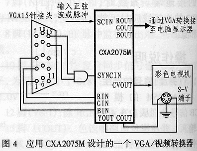
(5) An external resistor connected to the 75Ω driver output pin can prevent oscillation caused by dozens of picofarad capacitors between each pin.
(6) For YTRAP pin? Pin 17? The following three methods can be used to reduce the color confusion caused by the subcarrier frequency component in the Y signal. The first is to install a 30 ~ 68pF between YTRAP and GND Of capacitance. The second is to connect a capacitor and inductance in series between YARAP and GND. The third is to use the trap filter inside the chip.
5 Application circuit
Since China's color TV adopts the PA system, this article only lists the typical application circuit of the CXA 2075M using the PA internal trap mode (PAL IN-NAR TRAP mode). The specific circuit connection is shown in Figure 3.
Figure 4 is a VGA / video converter designed using CXA2075M. In the figure, the VGA 15-pin connector on the left can be connected to the VGA interface of the computer host graphics card. The output part can be connected to the TV through the video port or S terminal. The converter can also interface with computer monitors to achieve simultaneous display.

Follow WeChat

Download Audiophile APP

Follow the audiophile class
related suggestion
One. The market background is accompanied by the rapid development of computer and network technology, especially the increasing maturity of video codec technology and the rapid processing capacity of computers ...
Today, the custom-made IC and semiconductor IP leading OEM chip company announced the launch of Hantro G2 multi-format video decoding IP, supporting ...
In order to meet the actual needs of our country, this article on the basis of the DaVinci system hardware platform, using DaVinci software technology, proposed the development of digital movie screening ...

Digital high-definition video codec and video processing sample system is based on ARM's standard ARM11 processor, external standard 500Mega ...

This article makes an in-depth analysis of the filtering and storage modules in the H.264 decoder chip. And according to the characteristics of each time data for the corresponding memory ...

Committed to the design and development of integrated circuit chips and systems, Chengdu Guoteng Electronic Technology Co., Ltd. has launched a series of standard definition and high-definition video decoding, ...
This article takes OMAP3530 as an example, analyzes the hardware structure and software programming characteristics of the 0MAP platform; summarizes the special ...
TVP5150's low-power video decoding module rapidly increases with the demand for portable multimedia terminals, and has low power to the chip in video decoding ...
