Circuit principle analysis of electric bicycle charger
Electric bicycle charger
To supplement the energy of lead-acid batteries and nickel-cadmium batteries for electric vehicles, it is necessary to use a charger. There are many types of chargers. Generally, there are two types of power transformers. The high-power is generally used to ring the power frequency transformer. Although the efficiency is low, the current is large (up to 30A) and reliable. The freight electric three-wheeled use of it without exception, while the battery below 30Ah mostly uses switching power supply technology, which improves efficiency and eliminates the bulky power frequency transformer. The maximum charging current of electric bicycle chargers is mostly around 2A.
1. Electric bicycle charger with switching power supply technology
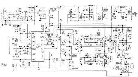
(1) Shandong GD36 charger
The circuit schematic is shown in Figure 12. The charger is a half-bridge charger. The main performance indicators are: input voltage: 170-260V; output voltage: 44 V (adjustable); maximum charging current: 1.8A; float charging current: 200 ~ 100mA.
1) Circuit principle
The charger circuit is mainly composed of mains rectification filtering, self-excited plus half-bridge conversion, PWM control, voltage control, current control, and output rectification filtering.
Rectifier filter mains 220V/50Hz through the diode D1 ~ D4 bridge rectification, capacitor C5 ~ C7 filter, get DC voltage of about 310V, as the power supply of the switching converter.
The self-excited and stimulated half-bridge output circuit is mainly composed of Q1, Q2, B2, B3 and other components.
Self-excited startup of the circuit is characterized by self-excited startup, the auxiliary power required by the control circuit is provided by itself, no need to set it separately. Self-oscillation is generated by the saturation characteristics of the core. The specific process is: turn on the power supply, and the 150V voltage on C5 and C6 provides the base bias voltage to the switching transistors Q1 and Q2 via R5, R7, R9, and R10. Let Q1 be biased by TR5 and micro-conducting, then push the 2-4 winding of transformer B2 to induce the polarity of pin 2 is positive and pin 4 negative, so 1-2 winding induces 1 pin positive and 2 pin negative voltage. It is applied to the emitter of Q1 to accelerate the conduction of Q1. This is a very strong positive feedback process, and Q1 quickly saturates. At the same time, the 3-5 winding induces a negative voltage of 3 feet and 5 feet, which makes Q2 cut off.
After Q1 is saturated, the 150 voltage charges the B31-2 main winding to store energy, and the current in the coil and the magnetic induction generated by it linearly increase with time. However, when the magnetic induction intensity increases to the saturation point Bm, the inductance decreases rapidly, and the collector current of Q1 increases sharply. The rate of increase is much greater than the increase of the base current, and Vce rises, so Q1 exits saturation and enters the amplification region. The induced voltage of the 2-4, 1-2, and 3-5 windings of the transformer B2 will be reversed. This is another strong positive feedback process, the result is Q1 cutoff, Q2 saturation conduction. Thereafter, this process is repeated to form an oscillation.
The working principle is as follows:
He oscillates: During the self-oscillation process, the secondary output voltage of B3 is full-wave rectified by D9 and D10, and C19 is filtered to establish the working power required for the PWM control circuit chip TL494. The TL494 starts to work, and Q3 and Q4 output PWM pulses with a phase difference of 180°, which are induced to 1-2 or 3-5 windings through the B26-7 and 7-8 windings. Then Q1 and Q2 turn from self-excitation to turn-on conduction under the driving of the PWM pulse. The output voltage of the secondary 9-7 and 9-8 windings of B3 is fully rectified by D15 and C21 filtered to obtain +44V voltage to charge the battery.
D6 and D7 are two clamp diodes to protect the switch tubes Q1 and Q2. The protection mechanism is to discharge the anti-excitation energy and leakage energy storage of the B3 primary and eliminate the anti-peak voltage. When Q1 is turned off and Q2 is not turned on, D7 is turned on, and the flyback energy is regenerated to C6 charging; when Q2 is turned off by conduction and Q1 is not yet turned on, D6 is turned on, The flyback energy regeneration charges the C5. Thus, on the one hand, the anti-peak voltage is eliminated, and on the other hand, the efficiency of the power supply is greatly improved by the return of the flyback energy to the power supply.
PWM control is composed of TL494. C12 and R19 form an oscillation with the internal circuit. When the parameters of the two RC components are icon values, the oscillation frequency is about 50 kHz. (13) The pin is connected to +5V, and the pulse output mode is set to push-pull output. 8. The push-pull widening pulse of the (11) pin output is amplified by the driving circuit and sent to the half-bridge output stage to control the turn-on of Q1 and Q2.
The R20 and R24 voltage division values ​​set the potential of the 4th leg of the dead zone control terminal, and the maximum conduction duty ratio is limited to less than 45%. C18 is a slow-start capacitor. After the power is turned on, the voltage across C18 is zero, the potential of pin 4 is approximately +5V, and the output pulse duty is zero. With the charging of C18, the voltage of the 4-pin gradually decreases, the on-duty ratio gradually increases, and the output voltage is gradually controlled.
Voltage and current control: R2**R27 is a voltage negative feedback sampling resistor. R26 and R27 are divided. The output voltage is sampled and added to pin 1 of TL494 for voltage control. R3 is the current sampling resistor, and the sampling voltage is applied to the (15) pin of TL494 via R13 for current control. The essence of current control is also to control the output voltage.
Push-pull drive: consists of Q3, Q4, B2 and other components. This is a typical transformer push-pull power amplifier circuit. The functions of D11 and D14 are similar to those of D5 and D7, and protect Q3 and Q4, and return the B2 primary flyback energy to the power supply.
The charging status indication is mainly composed of components such as an operational amplifier LM358, LED1, and LED2. When the charging current is large, the voltage at the upper end of the current sampling resistor R3 is much lower than the ground potential, the potential of the 2 pin of the LM358 is lower than the potential of the 3 pin, the output of the 1 pin is high, the battery charging indicator LED1 is lit; when the charging current is small (less than 200mA), +5V is divided by R36, R30, R3, the voltage at the upper end of R3 is slightly higher than the ground potential, the potential of LM3582 is higher than 3 feet, the output of 1 pin is low level, the battery charging indicator LED1 is off, 7 feet Output high level. LED2 is lit after being fully charged. During a certain period of charging, there is a transition state in which LED1 and LED2 are simultaneously lit.
2) Debugging
The output voltage is open and the output voltage is 44V. Change R26 or R27 to calibrate this value. The summer voltage should be 1V lower than 44V. If the voltage of the gel battery is lower, it may be charged.
When the output current is short-circuited, the output current is 1.8A. Change R13 to calibrate this value.
Status indication Debugging When the charging current is 200mA, the battery full indicator LED2 should start to light. Change R30 to calibrate this state.
3) Summary
Many half-bridge chargers, with TL494 as the core, have a very similar structure. The TL494 contains basic unit circuits such as oscillation, sawtooth waveform formation, PWM, and op amp. Regulator and current limit feedback are added to the op amp. In addition, a comparator integrated circuit is used for current segmentation control. These integrated circuit operations require power supply, power-on start, and startup circuit operation to supply power to them. Then, the auxiliary power supply gradually establishes a stable power supply to provide work for these integrated circuits. energy.
Some of these chargers have similar faults, such as a lower output voltage with no load and a lost output with load. Most of them are damaged by TL494, or the power supply circuit is faulty. The no-load output indicates that the self-excitation is normal, but the normal control system is not established. The self-excited condition with load is destroyed and the output voltage disappears.
For a half-bridge charger without any output at no load, in the case of damage to the fuse, first suspect whether the two switches are broken. When replacing the NPN tube, check whether the peripheral components such as 2.2Ω are damaged. After the parts are replaced, the power is checked, and it is still empty. However, an ordinary 100W incandescent bulb should be connected in series with the mains input. When the power is turned on, the incandescent bulb will flash and dim, and the half-bridge charger will be illuminated normally. , the description is basically repaired, and other items can be carried out; if the incandescent light bulb is always bright and not dark, the charger has other faults.
The reason for the damage of one type of switch tube is that the TL494 is intact, and the forward channel is backward until the switch tube is normal. However, there is a problem with the regulated feedback system. The pulse duty ratio of the TL494 output to the switch tube is out of control (increased), causing damage to the switch tube. Therefore, it is better to supply the integrated circuit with a regulated power supply after changing the switch tube, simulate changing the feedback voltage of the voltage feedback feedback system, and observe whether the duty cycle changes correspondingly with an oscilloscope.
It is very important to repair the safety of the charger. It is necessary to find out where the mains supply is in the circuit, where to take the mains and then do not touch the internal lines and parts. When testing with a multimeter, unplug the battery and the mains plug, discharge the capacitor, and discharge the filter capacitor with an ordinary incandescent bulb.
The adjustment of the charger is very important and directly affects the battery life. Taking a 12V battery as an example, the floating charging voltage of 13.5V~13.9V can be carried out for a long time. Generally, the output voltage should not exceed 14.2V, otherwise the battery will lose water. Need to be reminded: the pressure of the gel battery should be lower when controlling the charging voltage; the summer voltage should be lower, the reduction is about 4 square meters per °C for each cell (12V for 12V battery). The key to repairing the charger is to find the voltage sampling resistor with negative voltage feedback. Proficiency in reducing the resistance value of the upper part of the sampling resistor, the output voltage is reduced; increasing the resistance value of the upper part of the sampling resistor, the output voltage is increased. Or conversely, reduce the resistance value of the lower half of the sampling resistor, increase the output voltage; increase the resistance value of the lower half of the sampling resistor, and reduce the output voltage. The second is to find the charging current sampling resistor, as well as the current detection comparator, to master the method of changing the charging current in each stage.
The reference ground potential is important when analyzing the current sense comparator circuit. This is because the integrated circuit of the charger current sense comparator is powered by a single power supply, one end of the comparator is grounded, the other end of the comparator is connected to the sampling resistor, and the voltage on the sampling resistor is generally a negative voltage.
(2) Single-excitation charger of a company in Shijiazhuang
The schematic of the charger is shown in Figure 13. The single-excitation charger startup circuit is different from the half-bridge type. It is generally taken directly from the smooth DC power after the mains rectification and filtering. The integrated circuit is also mainly UC3842, UC3845 and UC3844N. There is also a three-terminal switch type TOP226 integrated with a more compact circuit. Block, UC38xx is a current-controlled PWM single-output dedicated chip. Widely used in power supply products such as computer monitor power supplies and electric vehicle chargers.
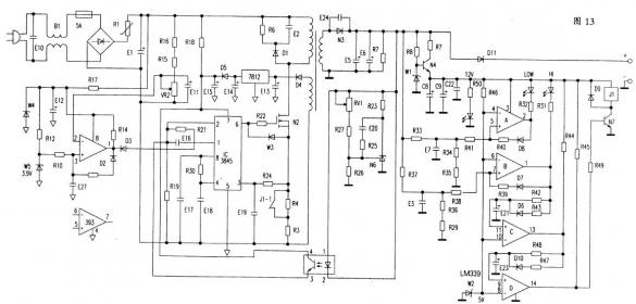
Similar to the TL494, the UC38xx contains an internal circuit necessary for the PWM dedicated chip such as an oscillator (OSC), error amplifier, pulse width modulation (PWM), and reference voltage generation. It also has three features, totem pole output circuit, output current up to 1A, can directly drive the power switch VDMOS tube: with an internal adjustable reference power supply. Undervoltage lockout can be performed; this locked PWM can be pulse-by-pulse current limit, also called weekly (period) limit.
In Fig. 13, R18, D5, N5, etc. constitute a start-up and power supply circuit. Power on instantly. The smoothed DC power after the mains rectification and filtering is applied to the UC38457 pin through R18 to start the power supply. At this time, D5 is reverse biased. After the UC3845 works, the windings of the switching transformer have induced voltage. The secondary winding voltage is regulated by D4 for N5 to regulate, and D5 is turned on to provide a stable working voltage for the UC3845 to complete startup and power supply. In the figure, LM393 is a deformed Schmitt voltage comparator used as mains overvoltage protection. When the mains is overvoltage, the comparator flips, pin 1 is low, and D3 turns on to turn off UC3845. The output-regulated negative feedback system consists of a photocoupler, a reference power supply N6, RV1, R27, R26, R23, and the like. Voltage regulation process: When the output voltage rises for some reason, the current flowing through the photocoupler LED increases, the light intensity increases, and the photocoupler phototransistor intensifies conduction. The internal resistance is reduced, so that the voltage of pin 2 of UC3845 rises, the PWM duty cycle is reduced, and the output voltage is pulled down. Conversely, increasing the PWM duty cycle and pulling the output voltage high will automatically stabilize the output voltage.
1) Overcurrent (overload) protection
The overcurrent signal of the switch tube is taken from the resistors R3 and R4. Once the switch tube is overcurrent, the voltage of pin 3 of UC3845 exceeds 1V, and the internal circuit will turn off the output to realize overcurrent (also called overload) protection. Increasing the sampling resistance is to reduce the operating point of the starting current, and the power output power is also reduced accordingly.
2) Overvoltage protection
The LM339 four voltage comparators A, B, C, and D of the power supply output are fixed at +5V. A and B detect the output voltage. When the output voltage is low, the initial stage of charging, A's 2 pin is low level, low voltage light LOW is bright, B's 1 foot is also low level, high voltage light HI is also bright; When the charging voltage rises. A flips, the low voltage lamp LOW goes out, the high voltage lamp HI continues to light, when the battery will be full, the battery voltage rises, B flips, 1 pin is high level, and the high pressure lamp HI goes out. At the same time, the (13) pin of C is high level, the (14) pin of D is also high level, N7 is turned on, J1 is connected, J1-1 (normally closed) is disconnected, and the sampling resistor R4 is connected. The current sampling resistor is turned on, and the starting current is controlled to lower the output current, and the floating charging phase is entered. N4, W1, R8, and R7 form a 12V regulated power supply, providing power for a 12V relay.
(3) Tianneng TN-1 intelligent negative pulse charger
Figure 14 is a circuit diagram of the Tianneng TN-1 intelligent negative pulse charger. The main part of this charger is a typical half-bridge two-stage charger, which is basically the same as the charger shown in Figure 12. Here we mainly introduce the working principle of the negative pulse charging part. This part of the circuit consists of three parts: discharge switch, negative pulse loading control and pulse oscillator.
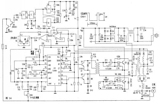
The discharge switch is a transistor Q6, Q6 is turned on, its collector and emitter short circuit the battery, the battery is discharged. The Q6 is cut off and the battery is restored. Q5 and Q6 are direct couplings, commonly known as Darlington tubes. Q6 is controlled by the combined negative pulse control and oscillator. The load negative pulse control consists of C3 and D of IC3. D is connected to the inverter (in the circuit, the NAND gate is connected in parallel as a non-gate). Only when the two inputs of C are high, the 3 pin is low, and the D is inverted to make the Q6 Pass, discharge the battery. The 2 pin of C comes from the multi-vibrator 1 (pulse width 3ms) positive pulse, the C pin 1 comes from the 1st pin of the two-phase current detecting circuit IC2, and the 1 pin is high level during the constant current charging. At this point, the negative pulse only works.
The pulse oscillator consists of IC3's A and B and C24, C25, and two 100kΩ resistors. It has a typical multi-harmonic oscillator with different charge and discharge time constants, high level 3ms, low level 1250ms. Negative pulse charging can improve the charging acceptance and lower the charging temperature. There is also a way to eliminate the problem of vulcanization and prolong the life of the battery. When the above charger is discharged, the charging circuit is not turned off.
2. Electric bicycle charger with power frequency transformer
(1) Happy brand KLG smart charger
Happy KLG Smart Charger is a high-powered charger with a ring-neck transformer that is commonly used in freight three-wheel drive. The circuit schematic is shown in Figure 15.
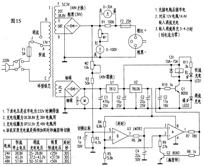
The transformer T has a tap on the primary. The secondary has two independent windings. The lower 14V is the auxiliary power winding. It supplies power to the control circuit. The upper charging winding has a tap for charging the 36V battery. The upper side is for 48V battery (unused). When the mains is connected to the primary tap A through the relay normally closed contact J-1, it is a constant current charging position, and the output is 43.2V. When the normally open contact of the relay is connected to the primary upper end B, it is a trickle charging position, and the output is 37.5. V ~ 43.2V.
U3 and G2 form a hysteresis battery voltage detection circuit. The battery voltage is applied to the 5 pin of U3B through voltage sampling resistors W2, R2 and R3. When the battery voltage rises to 43.2v, U3B flips, 7 pin outputs high level, U3A flips. Its 1 pin outputs a high level, which causes G2 to turn on, causing the U3 reference potential to drop, resulting in a hysteresis latch-up effect. At this time, since the 1 pin of U3A outputs a high level, G1 is turned on, the relay J is energized, and the normally open contact of the relay is connected to the point B, and enters the trickle charging position, and the output is 37.5V to 43.2V. Adjusting W2 can change the switching voltage. R6 and C6 are integration circuits with a delay of about one minute.
When the charger is used to charge a 48V battery, only two changes are needed: the charging main winding is switched from the tap to the upper end; the upper part of the voltage sampling resistor is increased. Replace the voltmeter if necessary.
Z18 Bone Conduction Headphones
Z18 Bone Conduction Headphones,Bone Conduction Headphones Gaming,Wireless Sports Headset,Outdoor Sports Bone Conducting Headset
Shenzhen Lonfine Innovation Technology Co., Ltd , https://www.lonfinesmart.com