In the design and layout of electronic equipment and communication systems, crystal oscillators and peripheral circuits must be carefully considered to optimize performance. As the core of the signal source, the crystal oscillator must produce a very high precision output, so it is very sensitive to high frequency noise from other boards.
This kind of circuit needs clear attention when designing. These technical instructions are design guidelines for reducing noise in some peripheral circuits. In these circuits, high-frequency noise is particularly beneficial to the output of the crystal oscillator.
Noise source
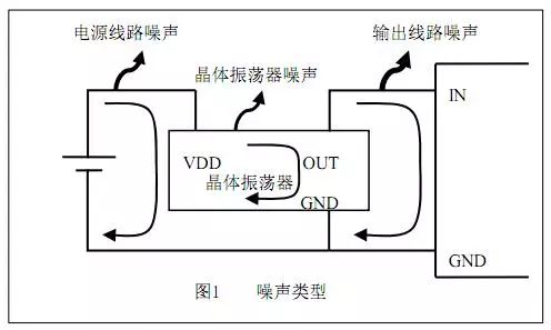
First, in Figure 1, we point out the typical noise generated by the crystal oscillator and peripheral circuits.
There are three main sources of noise:
1. Power line noise
2. Output line noise
3. The noise of the crystal oscillator
What is often referred to as "noise" is the cumulative result of these three factors.
Below we will explain the noise of the address type.
1. Power line noise
Voltage ripple and switching noise are usually emitted by power lines. This noise will affect the output of the crystal oscillator. In addition, it is necessary to ensure that the ripple noise generated by the crystal oscillator does not flow onto the power line. Implementing these measures can also improve isolation and prevent external noise generated by other devices from flowing into the crystal oscillator, thereby ensuring the stability of the crystal oscillator.
2. Output line noise
The output line noise refers to the signal output by the crystal oscillator of the output line as an antenna. For output signals and physical tracking, techniques to reduce noise should be implemented.
3. Crystal oscillator noise
The noise of the crystal oscillator refers to the noise emitted by the internal integrated circuit and circuit of the crystal oscillator. To solve this noise, it is necessary to ensure a stable power supply of the crystal oscillator and ensure the formation of the required waveform to achieve stable operation of the crystal oscillator.
These noise sources depend on the above-mentioned reasons and can be indirectly mitigated by the power line and output line technology mentioned later in this article.
The noise level emitted by the above-mentioned power supply is proportional to the current and the current loop path. Therefore, the reduction of current or current loop impedance will result in a reduction of emission noise. Generally speaking, the current and current loop path length are related to the crystal oscillator and its peripheral circuits.
Amount of current: power line = crystal oscillator> output line
Current loop size: output line>power line>crystal oscillator
The output line noise has the greatest impact on the crystal oscillator circuit, followed by the noise contribution from the power line. The noise emitted by the actual crystal oscillator is much lower than the noise from the other two sources.
Noise countermeasures
In these technical notes, we have studied the sources of noise in the crystal oscillator and its peripheral circuits. Here, we explain measures to reduce noise. There are three main noise reduction measures:
1. Establish a stable power and ground connection.
2. Install a filter to prevent noise from the power line.
3. Configure a stable output line on the motherboard.
1. Stable power and ground connection
Stable power supply and grounding refer to a very low impedance level in a wide frequency band (especially high frequency), and a conductor that achieves a uniform potential at all points of the bandwidth. In particular, the ground wire represents the basic potential of the circuit, so it must reach the maximum level of stability. This requires designing a ground plane with a wide surface area that does not shrink.
On multilayer boards, additional ground planes are used to configure power and ground wires on separate layers. When the design involves solder joints, a wider contact area ensures lower impedance and therefore less noise.
2. Power line filter
Usually, a filter is placed between the power line and the ground line to prevent the noise of the crystal oscillator from leaking to the power or ground line, and vice versa, to prevent the noise of the power line from entering the crystal oscillator. Generally, bypass capacitors are used as filters for power lines and ground lines. A detailed explanation is provided below.
A. Bypass capacitor
Bypass capacitors can reduce the impedance of the interaction, and help stabilize the operation of the circuit, while absorbing the noise that exists on the power line. This is a well-known noise reduction method. Installing capacitors with proper capacitance values ​​will solve most of the noise-related problems.
I. Bypass capacitor capacity value
The standard bypass capacitor value is between 0.01μF and 1μF. This value should be as low as possible, but within the frequency range of the power supply terminal VCC and the power line impedance relative to the ground, it is three times the crystal oscillator frequency. Here, you must confirm the frequency characteristics of this frequency to ensure that the impedance level on the high-frequency side or the low-band side does not increase.
II. Install bypass capacitor
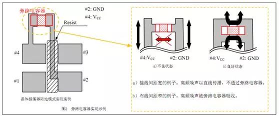
In order to reduce noise, the bypass capacitor should be installed as close to the crystal oscillator as possible. As the track length increases, the parasitic inductance will increase and cause higher frequency impedance to increase. The tracking length of the bypass capacitor should be configured so that the signal is connected to the power line through. This will force the noise to pass through the bypass capacitor and improve the noise cancellation effect.
Avoid the type shown in Figure 2a. When installing a bypass capacitor. High-frequency noise usually propagates in a straight line, so if the pattern shown in Figure 2a is used, the noise will not pass through the bypass capacitor. Therefore, the pattern shown in Figure 2b is used.
III. Configure a stable output line
The stable output line means that it can effectively convert the output waveform of the crystal oscillator into the required input signal, and has the smallest distortion and electromagnetic radiation. The key to configuring a stable output line is to ensure the required waveform attributes for the input, such as tr, tf, VOH, VOL, etc.
In addition, a stable output line needs to eliminate unnecessary signals, such as overshoot, low shot, ringing and echo, as shown in Figure 3b. In order to reduce unnecessary radiation, it is also important to understand the tracking antenna efficiency.
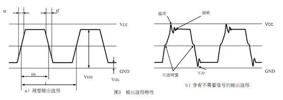
Measures to prevent distortion of the output waveform include:
a. Configure series resistance
b. Configure terminal resistance
c. Configure filter
d. Match output line impedance
a. Configure series resistance
Connecting a crystal oscillator input device usually results in waveform distortion, including overshoot, undershoot and ringing. These distorted high-frequency components, 3-7 times the oscillation frequency and generate noise, should be cancelled.
In order to eliminate this kind of distortion, a series resistor is connected between the output terminal of the crystal oscillator and the output line, as shown in Figure 4. The resistance value can make the sum (RO) and series resistance (RS) of the crystal oscillator's output impedance equal to the output line impedance (Z0).
A test can be performed to determine the best value of the series resistance. The test method includes measuring the output waveform with an oscilloscope and converting the series resistance from low to high value. The optimal resistance value means that the values ​​of overshoot, undershoot, and ringing are eliminated.

b. Configure terminal resistance
The configuration of the terminating resistor largely depends on the type of interface and the type of clock line used. The configuration will vary based on these factors.
Generally speaking, when the impedance on the output line does not match the impedance of the device input, the output waveform will be distorted. When the impedance does not match, the traveling wave cannot be fully received, and part of the signal is reflected back to the oscillator, resulting in distortion of the output waveform. This causes high frequency noise.
When the branched crystal oscillator is output to multiple devices, this waveform distortion can cause trigger errors. Therefore, correct termination and impedance matching are essential.
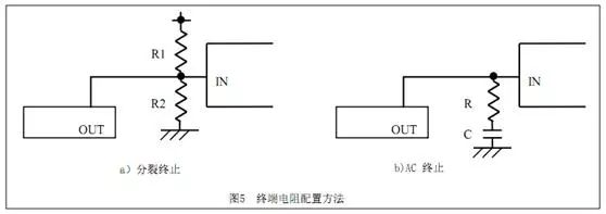
In order to prevent the echo from the receiving device, the impedance value of the input terminal and the output line should be the same. Figure 5 shows two common termination methods: split termination and AC termination.
c. Configure filter
Usually, the output waveform distortion can be solved by series resistance or terminal resistance. Use filtering when these methods do not solve the problem. The use of filters is an effective way to eliminate high-frequency noise, but this method will lead to an increase in TR and TF (waveform dissipation).
Therefore, you must select a filter suitable for the attributes of TR and TF. In addition, using a larger capacitor as a filter can lead to an increase in current, and vice versa, it will lead to an increase in noise.
d. Output line impedance matching
Reducing the waveform echo on the output line requires the output line impedance to be as consistent as possible. As shown in Figure 6, achieving consistent output line impedance involves the output line pattern curve configuration that converts the right angle to a 45º angle or, if possible, a circular curve. In addition, avoid the use of through holes or T-shapes.
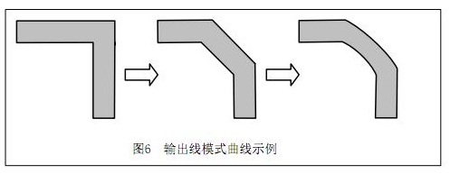
Finally, we will introduce the two most important ways to reduce noise emissions.
a. Use a shorter output line
In all circuits, the output line is the most prone to noise. Therefore, in design and layout, priority should be given to allowing the shortest output line to not appear impedance fluctuations. Use shorter wiring to move the output line resonant frequency to the high-frequency side. The higher the frequency, the more damping of the output frequency components will result in a reduction in noise.
b. Use a shorter current loop path
As mentioned above, the noise level emitted by the output line is proportional to the current loop path length. Therefore, it is important that the output and ground traces of the crystal oscillator and input devices should be as short as possible. An easy way to achieve this is to install the ground plane on the opposite side of the output trace.
As mentioned above, careful circuit design of the crystal oscillator and its peripheral circuits is the key to reducing noise. The best circuit design can avoid noise-related problems and enable the device to fully realize its performance potential.
What is an Explosion-proof Screen Protector?
Now Mobile Phone Screen Protector can be seen everywhere in our daily life. The most common one should be "Tempered Glass Screen Protector", but I'm still relatively unfamiliar with "Explosion-proof Screen Protector for mobile phones". Next, I will briefly introduce Explosion-proof Screen Protective Film. membrane.
The Mobile Phone Explosion-proof Screen Protector is mainly made of imported PET material and a layer of silicone coating. Since the thickness of the silicone coating is thicker than that of ordinary screen protectors, it can decompose external force under strong collision to buffer the impact and prevent the mobile phone from being accidentally hit. The glass panel of the mobile phone is broken and scattered, which reduces the hidden damage of the glass panel and ensures the safety of users. That is to say, "Mobile Phone Explosion-proof Screen Protector" is not to prevent the phone screen from exploding, but to prevent the phone screen from being impacted, it can decompose the external force and reduce the chance of the phone screen breaking. The anti-impact, anti-scratch, anti-wear, etc. of the mobile phone Explosion-proof Protective Film can protect the screen to a certain extent compared to the general PET and PE Mobile Phone Screen Protectors.
Anti-Explossion HD Films,Anti-Scratch Protective Film,Anti-Wear Screen Protector,Scratch-Resistant Screen Film
Shenzhen TUOLI Electronic Technology Co., Ltd. , https://www.szhydrogelprotector.com