Abstract: This article introduces Dallas Semiconductor's improved technology for traditional 8051 microcontrollers, creating pin-compatible high-performance alternatives that can reach 33 MIP speeds. In addition, it also includes multiple data pointers, extended memory addressing (up to 16MB) and flash memory, greatly improving the speed and effectiveness of the device.
System designers know that microcontrollers are the heart of all embedded systems—the source of various system activities. Over the past 18 years, Dallas Semiconductor (a wholly-owned subsidiary of Maxim Integrated Products) has redefined the ubiquitous 8051 microcontroller. Perhaps the biggest improvement to the microcontroller in the past decade is in the speed at which it executes instructions. Our single-cycle processors have reached exciting performance goals—one clock per machine cycle, currently 33 million instructions per second (MIPS). Based on this core, our family of security, network, and mixed-signal 8051 microcontrollers has always been an industry model in terms of functional integration and innovation.
Why build the innovative microcontroller family on the old 8051 instruction set? The reason is simple because it is one of the most popular 8-bit microcontroller architectures in the world. This instruction set is simple and easy to understand, and it is popular with designers of embedded systems. Many instructions can directly access the I / O pins, which facilitates rapid operation (bit manipulation) of peripheral devices. A wide variety of on-chip peripherals has almost unlimited combinations. In addition, development tools for the 8051 microcontroller family can be found everywhere, so that you can start an application development very easily and without high cost.
Security and Confidentiality In 1987, Dallas Semiconductor / Maxim introduced the DS5000T, an independently developed new microcontroller based on the 8051 instruction set and function set. To provide new performance and advantages, engineers built their designs on non-volatile SRAM technology rather than traditional EPROM. Relying on its leading low-power technology, memory partitions and battery backup circuits are directly integrated into the microcontroller chip. The main advantage of this system is its speed. The write operation of other types of non-volatile memory is usually very slow, but the non-volatile SRAM can be read and written in a single cycle at a very high speed. This is ideal for high-speed, non-volatile data acquisition applications, which often require real-time data capture. Together with an external SRAM and battery, a complete microcontroller system is formed, with up to 64kB of non-volatile program and data storage space.
Thanks to non-volatile SRAM technology, both data and program memory can be reprogrammed in the system, allowing byte-by-byte, running programming. In a standard microcontroller system, to reprogram, the program memory must be removed from the system (EPROM), or block erase, and memory access (flash) is prohibited during the erase process. The programming of the microcontroller based on non-volatile SRAM is very easy and fast, and it can be programmed through a serial port using a PC or a dedicated programmer. The bootstrap loader resident in the ROM directly downloads the program or data to the microcontroller for fast debugging or on-site upgrade.
The unique advantages of non-volatile SRAM provide a new method for the security of system firmware. Since the bootstrap loader fully controls the loading of the program to the non-volatile SRAM, we use a 40-bit or 80-bit encryption key to encrypt the address and data bus. Any program or data loaded into the microcontroller is automatically encrypted before being stored in the SRAM. This encryption method can prevent hackers from stealing programs or data in the microcontroller. During the execution of the instruction, the microcontroller takes out the encrypted operation code and completes the decryption and execution in one machine cycle. The use of non-volatile SRAM allows read / write access at full speed, and instruction decryption does not cause any delay.
These security features have reached the extreme in the DS5250, which is a secure 8051 microcontroller that is widely used in financial terminals and payment systems around the world. This anti-attack microcontroller integrates a 4-clock machine cycle core and enhanced triple-DES encryption logic for program memory encryption. In addition, intrusion detection and on-chip tamper detection are added, and the memory is automatically erased once tampering is detected. An internal microprobe shield prevents tampering with the wafer. Also, non-volatile SRAM is the best choice for applications that require a high degree of security. Because it can write at high speed, the microcontroller can quickly erase confidential information and sensitive data, which is better than any other type of memory.
The DS5250 is the only microcontroller that provides the highest level of security while running every instruction at full speed.
The high-speed, low-power 8051 processor core has been basically stagnant since its birth (from the late 1970s to the 1980s), but this is not the case with embedded systems. By adding new software features and peripheral devices, system designers have continuously improved and upgraded their 8051-based applications. This "function spread" pushes the existing 8051 performance to the limit. Unfortunately, the improvements to the 8051 core have not kept pace. It seems that system designers have to switch to other processors and spend a lot of money to redesign and update their systems.
The performance bottleneck is the outdated 8051 microcontroller processing core that was born in the 1970s. Although the speed of the external crystal oscillator is close to 40MHz, the traditional 8051 still requires 12 clocks to run a machine cycle. Each instruction requires 1 to 4 machine cycles, which means that the execution of an instruction requires as little as 12 or 48 clock cycles. In this way, the throughput rate is limited to only 3MIPS, even when running a series of single-cycle instructions like NOP (Figure 1).
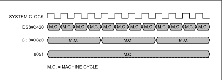
Figure 1. Due to the reduction in the number of clocks required per machine cycle, the performance of the same instruction set has increased by more than three times (compared to 12 clocks, 4 clocks, and 1 clock per machine cycle).
In 1991, we began to redesign the 8051 microcontroller in order to achieve a breakthrough in performance. The design team first analyzed the traditional 8051 design. We found that there was a huge waste in the original 12 clock per machine cycle architecture: most instructions were forced to execute dummy cycles. The engineers completely refactored the CPU, requiring only 4 clocks per machine cycle instead of 12. The second internal data bus eliminates structural bottlenecks that hinder performance. The high-power I / O driver improves the conversion speed of the port line when accessing external memory. All built-in peripherals, such as timers and serial ports, run at higher clock frequencies. However, at every step on this path to change, there is an absolutely unchanged criterion-the instruction set must maintain compatibility with the 8051 instruction set opcode.
In the end, a brand-new 8051-based microcontroller was born, which increased the efficiency of the core by three times compared to the original 8051. At the same frequency, the running speed of most instructions increased by three times. In addition to the improved core efficiency, the maximum external oscillation frequency of most devices has also been increased to 33MHz or 40MHz. System designers plagued by the ancient, low-speed 8051 can now easily upgrade their systems to speeds up to 10 MIPS without modifying the software.
In addition to speed improvements, the redesigned core also brings another benefit: lower power consumption. Basic physical laws tell us that the power consumption of a digital circuit is proportional to the number of transistors that have switching actions and the rate (frequency) of switching. Because the new core uses fewer oscillation cycles per machine cycle, the energy required to execute each instruction is significantly reduced compared to the traditional 8051.
In addition, a special power management mode can temporarily reduce the power consumption of the microcontroller through a software-configurable internal clock divider. By reducing the machine cycle rate from 4 clocks per machine cycle to 64 or 256 clocks per machine cycle, power consumption can be further reduced. The switchback function allows the device to return to divide-by-4 mode immediately after receiving an external interrupt or detecting a serial port start bit. This feature allows the device to maintain a low-power standby state when there is less work, and can quickly resume full-speed operation when necessary. Figure 2 shows the relative power consumption in different modes.
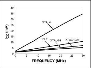
Figure 2. During the period of reduced workload, our power management mode consumes less current than the idle mode, and the CPU is still active.
Beyond 33MIPSDallas Semiconductor / Maxim began designing a new core in 1997 to achieve higher performance. Applications based on 8051 are constantly evolving, and users are calling for higher performance. The design team locked their goal at the pinnacle of performance: a new microcontroller that runs the 8051 instruction set, but has only one clock per machine cycle. Using a highly parallel architecture and a new manufacturing process, a pin-to-pin compatible, directly replacing the original 8051 design came out.
In the end, we launched the new DS89C430 / DS89C450—an ultra-high performance microcontroller with one clock per machine cycle, running at up to 33MIPS (Figure 3). These devices break through the original performance barriers and provide 16-bit performance at the price of an 8-bit microcontroller. These microcontrollers provide a variety of different bus addressing modes, allowing users to optimize the work of the processor according to specific application requirements. Most importantly, they maintain 100% compatibility with the 8051 instruction set. At the same time, they can run existing 8051 applications at a higher speed than any other 8051-based microcontroller.
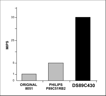
Figure 3. The performance of the DS89C430 33MIPS far exceeds that of its competitors.
In addition to the lightning-fast core, the DS89C430 / DS89C450 also integrates up to 64kB of flash memory that can be programmed in the system. The bootloader resident in the ROM allows the user to adjust the microcontroller code at any time, making the design very flexible. Unlike other microcontrollers that use proprietary or non-standard interfaces, the DS89C430's bootloader can be operated by a standard PC using any terminal emulation software through a serial port.
Han Xinbing, more benefits. If the programmer does not have enough memory address space to control, the speed advantage will be unavailable. The traditional 8051 uses a 16-bit memory bus to limit the memory space to within 64kB. For some applications, such limited storage space is sufficient. But as the application upgrades, the complexity and scale of the code expands rapidly, and we realize that this type of application requires a solution, while maintaining compatibility with 8051 as much as possible.
Some designers use partition switching to expand the addressing space. The I / O line is used as an address line in exchange for more storage space at the expense of some I / O resources. But this approach has two important flaws. First of all, the code must be segmented in units of 64kB or less, which is a very time-consuming task, because each time the code is adjusted, it must be segmented again. Second, every time the code crosses a section, a special software process must be used to switch the I / O lines. Because of this software overhead, the overall performance of the system will be reduced.
A better solution should be to equip the device with a wider address bus. This is the case with the DS80C400, which has a 24-bit address bus that can directly address 16MB of program memory and 16MB of data memory. The implementation of new functions does not rely on new opcodes outside the 8051 instruction set. Two bus modes are provided. The first page addressing mode uses advanced automatic partition switching technology, which greatly speeds up access to extended memory while maintaining compatibility with the binary code of the traditional 8051 compiler. The second continuous mode can transparently address the entire 16MB storage space, but requires the compiler to be able to generate the additional operands required for the 24-bit address. The larger address space allows larger programs to operate at higher speeds, opening up a wider application space for microcontrollers, such as large mathematical function libraries, lookup tables, and even Java ™ virtual machines, the latter of which has been The networked microcontrollers DS80C390 and DS80C400 are supported and become part of the Mini Internet Interface (TINI®) operating environment.
Every step along the way has a condition that must be followed—the instruction set must maintain compatibility with the 8051 instruction set opcode.
In order to avoid a new performance bottleneck, it is necessary to make long-term improvements to all aspects of the chip in order to avoid a new performance bottleneck. One of the most important improvements is the improvement for MOVX data storage access. The operation of the data memory is a very troublesome thing for the original 8051. To access a single byte in the MOVX memory, it takes several cycles to load a 16-bit data pointer before reading and writing the target address.
The DS89C430 maintains 100% compatibility with the 8051 instruction set, so it can directly run the original 8051 application while still being faster than any other 8051-based microcontroller.
The inefficiency of this kind of operation is particularly prominent when performing block copy operations, which require data to be transferred from one location in the MOVX memory to another location. In the block copy operation, the single data pointer must double as the source address and destination address pointer. In a traditional 8051 microcontroller, this operation is a complex, multi-step process: loading the source address into the data pointer. Increment or adjust the data pointer to point to the next unit. Take data from the MOVX memory to the accumulator. Save the source address to the register. Load the target address into the data pointer. Increment or adjust the data pointer to point to the next unit. The data is written into the MOVX memory by the accumulator. Save the target address to the register. The larger address space allows faster access to larger programs, such as the Java virtual machine supported by network microcontrollers.
You may have noticed that almost half of the steps in the above process are used to swap a single data pointer between the target and source addresses, which will prevent the overall performance. The solution is to add a second data pointer and allocate special registers for the source and destination pointers. With the second data pointer, many data operations can be done by hardware, reducing software overhead. The double data pointer can be accessed independently, and the data pointer currently selected when the MOVX instruction is executed can be selected through a special data pointer selection bit. With dual data pointers, the same block copy operation requires much fewer steps:
Only one initialization is required: The first data pointer is initialized to the source address. The second data pointer is initialized to the target address. Main loop: Take the data to the accumulator. Increment or adjust the first data pointer to point to the next cell. Select the second data pointer. The data is written into the MOVX memory by the accumulator. Increment or adjust the data pointer to point to the next unit. As can be seen from Figure 4, when using the 33MHz DS89C430 to execute a 1000-byte block copy routine, the use of dual data pointers eliminates the overhead of switching single data pointers, saving 33% of the running time. In the family of high-speed and ultra-high-speed microcontrollers, some members have added other optional data pointer enhancements. The auto-increment / decrement function (denoted as AID in Figure 4) automatically executes a MOVX-related instruction, and automatically increments or decrements the data pointer, eliminating the INC DPTR instruction. The automatic switching function (shown as TSL in FIG. 4) follows the MOVX related instructions to automatically switch the active data pointer, eliminating the need to switch data pointer instructions. Figure 4 also shows the relative time required to perform the same task when all these functions are adopted. Note that when all functions are enabled, the DS89C430 executes a 1000-byte block copy routine 103% faster than the original 8051 microcontroller.
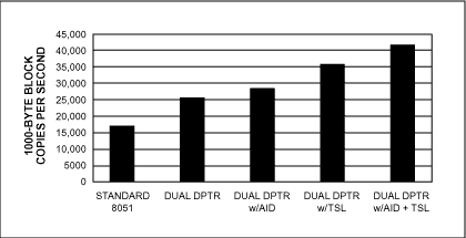
Figure 4. Dual data pointers increase the speed of block copy operations.
Prospects As applications require higher and higher speeds, Maxim is working hard to exceed one performance limit after another. Whether it is its faster stack access speed, extended addressing space, or basic processing speed, our microcontroller design can ultimately meet the various requirements of embedded system designers.
However, competitive design does not only require speed. More complex applications require more program space, so we are expanding the microcontroller series that directly replaces the original 8051 to 64kB flash memory. Our new product pipeline is designing more peripherals in order to enhance the capabilities of embedded systems while reducing board space requirements. The network microcontroller has some more advanced functions, including CAN, Ethernet, and 1-Wire® multi-level networking capabilities. The secure microcontroller has a hardware-implemented mathematical accelerator for the public key encryption system and quickly deletes the key when tampering is detected. Mixed-signal microcontrollers can process signals from the real world to achieve better terminal equipment.
Our pursuit of microcontroller performance goes beyond the 8051 core. One of our new series, the MAXQ® 16-bit RISC microcontroller, achieves a higher performance-to-power ratio. The path leading us to this goal is a single cycle instruction. Single-cycle instructions increase the instruction bandwidth, which can provide higher performance, and it is possible to reduce power consumption by reducing the clock frequency. Except for long jumps / long calls and access to certain extension registers, all MAXQ instructions are executed in a single clock cycle. Although many RISC microcontrollers claim to support single-cycle instructions, the fact is that only a portion of the instructions or addressing modes are single-cycle. In MAXQ, most of them are single-cycle instructions.
In addition, the MAXQ architecture improves clock cycle utilization because its single-cycle operation does not rely on instruction pipelines (common in many RISC microcontrollers). The hardware for decoding and executing MAXQ instructions is so simple (and fast) that they can be completed in the same clock cycle as the instruction fetch and have little effect on the maximum operating frequency. In order to illustrate the advantages of canceling the instruction pipeline, let's examine an ordinary RISC CPU with a pipeline structure. When encountering a program branch, the CPU needs one or more clock cycles (which varies depending on the pipeline depth) to turn the program to the target branch address and discard the fetched instructions. Obviously, using clock cycles for discarding instructions (rather than executing instructions) is a wasteful and unpleasant practice because it reduces performance and increases power consumption. Despite this unpleasant operation, the CPU stealing the clock to reinstall the pipeline is still an inevitable flaw in this architecture. A distinguishing feature of the MAXQ architecture that distinguishes it from other 8-bit and 16-bit RISC microcontrollers is that the execution of a single-cycle instruction does not depend on the instruction pipeline (which also avoids the problem of wasted clock cycles).
For more information on how to obtain the highest performance with the lowest power consumption, see the white paper "Teaching Old Dogs New Tricks: Improving the Power Efficiency of 8051-Based Designs" (English only).
System designers know that microcontrollers are the heart of all embedded systems—the source of various system activities. Over the past 18 years, Dallas Semiconductor (a wholly-owned subsidiary of Maxim Integrated Products) has redefined the ubiquitous 8051 microcontroller. Perhaps the biggest improvement to the microcontroller in the past decade is in the speed at which it executes instructions. Our single-cycle processors have reached exciting performance goals—one clock per machine cycle, currently 33 million instructions per second (MIPS). Based on this core, our family of security, network, and mixed-signal 8051 microcontrollers has always been an industry model in terms of functional integration and innovation.
Why build the innovative microcontroller family on the old 8051 instruction set? The reason is simple because it is one of the most popular 8-bit microcontroller architectures in the world. This instruction set is simple and easy to understand, and it is popular with designers of embedded systems. Many instructions can directly access the I / O pins, which facilitates rapid operation (bit manipulation) of peripheral devices. A wide variety of on-chip peripherals has almost unlimited combinations. In addition, development tools for the 8051 microcontroller family can be found everywhere, so that you can start an application development very easily and without high cost.
Security and Confidentiality In 1987, Dallas Semiconductor / Maxim introduced the DS5000T, an independently developed new microcontroller based on the 8051 instruction set and function set. To provide new performance and advantages, engineers built their designs on non-volatile SRAM technology rather than traditional EPROM. Relying on its leading low-power technology, memory partitions and battery backup circuits are directly integrated into the microcontroller chip. The main advantage of this system is its speed. The write operation of other types of non-volatile memory is usually very slow, but the non-volatile SRAM can be read and written in a single cycle at a very high speed. This is ideal for high-speed, non-volatile data acquisition applications, which often require real-time data capture. Together with an external SRAM and battery, a complete microcontroller system is formed, with up to 64kB of non-volatile program and data storage space.
Thanks to non-volatile SRAM technology, both data and program memory can be reprogrammed in the system, allowing byte-by-byte, running programming. In a standard microcontroller system, to reprogram, the program memory must be removed from the system (EPROM), or block erase, and memory access (flash) is prohibited during the erase process. The programming of the microcontroller based on non-volatile SRAM is very easy and fast, and it can be programmed through a serial port using a PC or a dedicated programmer. The bootstrap loader resident in the ROM directly downloads the program or data to the microcontroller for fast debugging or on-site upgrade.
The unique advantages of non-volatile SRAM provide a new method for the security of system firmware. Since the bootstrap loader fully controls the loading of the program to the non-volatile SRAM, we use a 40-bit or 80-bit encryption key to encrypt the address and data bus. Any program or data loaded into the microcontroller is automatically encrypted before being stored in the SRAM. This encryption method can prevent hackers from stealing programs or data in the microcontroller. During the execution of the instruction, the microcontroller takes out the encrypted operation code and completes the decryption and execution in one machine cycle. The use of non-volatile SRAM allows read / write access at full speed, and instruction decryption does not cause any delay.
These security features have reached the extreme in the DS5250, which is a secure 8051 microcontroller that is widely used in financial terminals and payment systems around the world. This anti-attack microcontroller integrates a 4-clock machine cycle core and enhanced triple-DES encryption logic for program memory encryption. In addition, intrusion detection and on-chip tamper detection are added, and the memory is automatically erased once tampering is detected. An internal microprobe shield prevents tampering with the wafer. Also, non-volatile SRAM is the best choice for applications that require a high degree of security. Because it can write at high speed, the microcontroller can quickly erase confidential information and sensitive data, which is better than any other type of memory.
The DS5250 is the only microcontroller that provides the highest level of security while running every instruction at full speed.
The high-speed, low-power 8051 processor core has been basically stagnant since its birth (from the late 1970s to the 1980s), but this is not the case with embedded systems. By adding new software features and peripheral devices, system designers have continuously improved and upgraded their 8051-based applications. This "function spread" pushes the existing 8051 performance to the limit. Unfortunately, the improvements to the 8051 core have not kept pace. It seems that system designers have to switch to other processors and spend a lot of money to redesign and update their systems.
The performance bottleneck is the outdated 8051 microcontroller processing core that was born in the 1970s. Although the speed of the external crystal oscillator is close to 40MHz, the traditional 8051 still requires 12 clocks to run a machine cycle. Each instruction requires 1 to 4 machine cycles, which means that the execution of an instruction requires as little as 12 or 48 clock cycles. In this way, the throughput rate is limited to only 3MIPS, even when running a series of single-cycle instructions like NOP (Figure 1).
Figure 1. Due to the reduction in the number of clocks required per machine cycle, the performance of the same instruction set has increased by more than three times (compared to 12 clocks, 4 clocks, and 1 clock per machine cycle).
In 1991, we began to redesign the 8051 microcontroller in order to achieve a breakthrough in performance. The design team first analyzed the traditional 8051 design. We found that there was a huge waste in the original 12 clock per machine cycle architecture: most instructions were forced to execute dummy cycles. The engineers completely refactored the CPU, requiring only 4 clocks per machine cycle instead of 12. The second internal data bus eliminates structural bottlenecks that hinder performance. The high-power I / O driver improves the conversion speed of the port line when accessing external memory. All built-in peripherals, such as timers and serial ports, run at higher clock frequencies. However, at every step on this path to change, there is an absolutely unchanged criterion-the instruction set must maintain compatibility with the 8051 instruction set opcode.
In the end, a brand-new 8051-based microcontroller was born, which increased the efficiency of the core by three times compared to the original 8051. At the same frequency, the running speed of most instructions increased by three times. In addition to the improved core efficiency, the maximum external oscillation frequency of most devices has also been increased to 33MHz or 40MHz. System designers plagued by the ancient, low-speed 8051 can now easily upgrade their systems to speeds up to 10 MIPS without modifying the software.
In addition to speed improvements, the redesigned core also brings another benefit: lower power consumption. Basic physical laws tell us that the power consumption of a digital circuit is proportional to the number of transistors that have switching actions and the rate (frequency) of switching. Because the new core uses fewer oscillation cycles per machine cycle, the energy required to execute each instruction is significantly reduced compared to the traditional 8051.
In addition, a special power management mode can temporarily reduce the power consumption of the microcontroller through a software-configurable internal clock divider. By reducing the machine cycle rate from 4 clocks per machine cycle to 64 or 256 clocks per machine cycle, power consumption can be further reduced. The switchback function allows the device to return to divide-by-4 mode immediately after receiving an external interrupt or detecting a serial port start bit. This feature allows the device to maintain a low-power standby state when there is less work, and can quickly resume full-speed operation when necessary. Figure 2 shows the relative power consumption in different modes.
Figure 2. During the period of reduced workload, our power management mode consumes less current than the idle mode, and the CPU is still active.
Beyond 33MIPSDallas Semiconductor / Maxim began designing a new core in 1997 to achieve higher performance. Applications based on 8051 are constantly evolving, and users are calling for higher performance. The design team locked their goal at the pinnacle of performance: a new microcontroller that runs the 8051 instruction set, but has only one clock per machine cycle. Using a highly parallel architecture and a new manufacturing process, a pin-to-pin compatible, directly replacing the original 8051 design came out.
In the end, we launched the new DS89C430 / DS89C450—an ultra-high performance microcontroller with one clock per machine cycle, running at up to 33MIPS (Figure 3). These devices break through the original performance barriers and provide 16-bit performance at the price of an 8-bit microcontroller. These microcontrollers provide a variety of different bus addressing modes, allowing users to optimize the work of the processor according to specific application requirements. Most importantly, they maintain 100% compatibility with the 8051 instruction set. At the same time, they can run existing 8051 applications at a higher speed than any other 8051-based microcontroller.
Figure 3. The performance of the DS89C430 33MIPS far exceeds that of its competitors.
In addition to the lightning-fast core, the DS89C430 / DS89C450 also integrates up to 64kB of flash memory that can be programmed in the system. The bootloader resident in the ROM allows the user to adjust the microcontroller code at any time, making the design very flexible. Unlike other microcontrollers that use proprietary or non-standard interfaces, the DS89C430's bootloader can be operated by a standard PC using any terminal emulation software through a serial port.
Han Xinbing, more benefits. If the programmer does not have enough memory address space to control, the speed advantage will be unavailable. The traditional 8051 uses a 16-bit memory bus to limit the memory space to within 64kB. For some applications, such limited storage space is sufficient. But as the application upgrades, the complexity and scale of the code expands rapidly, and we realize that this type of application requires a solution, while maintaining compatibility with 8051 as much as possible.
Some designers use partition switching to expand the addressing space. The I / O line is used as an address line in exchange for more storage space at the expense of some I / O resources. But this approach has two important flaws. First of all, the code must be segmented in units of 64kB or less, which is a very time-consuming task, because each time the code is adjusted, it must be segmented again. Second, every time the code crosses a section, a special software process must be used to switch the I / O lines. Because of this software overhead, the overall performance of the system will be reduced.
A better solution should be to equip the device with a wider address bus. This is the case with the DS80C400, which has a 24-bit address bus that can directly address 16MB of program memory and 16MB of data memory. The implementation of new functions does not rely on new opcodes outside the 8051 instruction set. Two bus modes are provided. The first page addressing mode uses advanced automatic partition switching technology, which greatly speeds up access to extended memory while maintaining compatibility with the binary code of the traditional 8051 compiler. The second continuous mode can transparently address the entire 16MB storage space, but requires the compiler to be able to generate the additional operands required for the 24-bit address. The larger address space allows larger programs to operate at higher speeds, opening up a wider application space for microcontrollers, such as large mathematical function libraries, lookup tables, and even Java ™ virtual machines, the latter of which has been The networked microcontrollers DS80C390 and DS80C400 are supported and become part of the Mini Internet Interface (TINI®) operating environment.
Every step along the way has a condition that must be followed—the instruction set must maintain compatibility with the 8051 instruction set opcode.
In order to avoid a new performance bottleneck, it is necessary to make long-term improvements to all aspects of the chip in order to avoid a new performance bottleneck. One of the most important improvements is the improvement for MOVX data storage access. The operation of the data memory is a very troublesome thing for the original 8051. To access a single byte in the MOVX memory, it takes several cycles to load a 16-bit data pointer before reading and writing the target address.
The DS89C430 maintains 100% compatibility with the 8051 instruction set, so it can directly run the original 8051 application while still being faster than any other 8051-based microcontroller.
The inefficiency of this kind of operation is particularly prominent when performing block copy operations, which require data to be transferred from one location in the MOVX memory to another location. In the block copy operation, the single data pointer must double as the source address and destination address pointer. In a traditional 8051 microcontroller, this operation is a complex, multi-step process: loading the source address into the data pointer. Increment or adjust the data pointer to point to the next unit. Take data from the MOVX memory to the accumulator. Save the source address to the register. Load the target address into the data pointer. Increment or adjust the data pointer to point to the next unit. The data is written into the MOVX memory by the accumulator. Save the target address to the register. The larger address space allows faster access to larger programs, such as the Java virtual machine supported by network microcontrollers.
You may have noticed that almost half of the steps in the above process are used to swap a single data pointer between the target and source addresses, which will prevent the overall performance. The solution is to add a second data pointer and allocate special registers for the source and destination pointers. With the second data pointer, many data operations can be done by hardware, reducing software overhead. The double data pointer can be accessed independently, and the data pointer currently selected when the MOVX instruction is executed can be selected through a special data pointer selection bit. With dual data pointers, the same block copy operation requires much fewer steps:
Only one initialization is required: The first data pointer is initialized to the source address. The second data pointer is initialized to the target address. Main loop: Take the data to the accumulator. Increment or adjust the first data pointer to point to the next cell. Select the second data pointer. The data is written into the MOVX memory by the accumulator. Increment or adjust the data pointer to point to the next unit. As can be seen from Figure 4, when using the 33MHz DS89C430 to execute a 1000-byte block copy routine, the use of dual data pointers eliminates the overhead of switching single data pointers, saving 33% of the running time. In the family of high-speed and ultra-high-speed microcontrollers, some members have added other optional data pointer enhancements. The auto-increment / decrement function (denoted as AID in Figure 4) automatically executes a MOVX-related instruction, and automatically increments or decrements the data pointer, eliminating the INC DPTR instruction. The automatic switching function (shown as TSL in FIG. 4) follows the MOVX related instructions to automatically switch the active data pointer, eliminating the need to switch data pointer instructions. Figure 4 also shows the relative time required to perform the same task when all these functions are adopted. Note that when all functions are enabled, the DS89C430 executes a 1000-byte block copy routine 103% faster than the original 8051 microcontroller.
Figure 4. Dual data pointers increase the speed of block copy operations.
Prospects As applications require higher and higher speeds, Maxim is working hard to exceed one performance limit after another. Whether it is its faster stack access speed, extended addressing space, or basic processing speed, our microcontroller design can ultimately meet the various requirements of embedded system designers.
However, competitive design does not only require speed. More complex applications require more program space, so we are expanding the microcontroller series that directly replaces the original 8051 to 64kB flash memory. Our new product pipeline is designing more peripherals in order to enhance the capabilities of embedded systems while reducing board space requirements. The network microcontroller has some more advanced functions, including CAN, Ethernet, and 1-Wire® multi-level networking capabilities. The secure microcontroller has a hardware-implemented mathematical accelerator for the public key encryption system and quickly deletes the key when tampering is detected. Mixed-signal microcontrollers can process signals from the real world to achieve better terminal equipment.
Our pursuit of microcontroller performance goes beyond the 8051 core. One of our new series, the MAXQ® 16-bit RISC microcontroller, achieves a higher performance-to-power ratio. The path leading us to this goal is a single cycle instruction. Single-cycle instructions increase the instruction bandwidth, which can provide higher performance, and it is possible to reduce power consumption by reducing the clock frequency. Except for long jumps / long calls and access to certain extension registers, all MAXQ instructions are executed in a single clock cycle. Although many RISC microcontrollers claim to support single-cycle instructions, the fact is that only a portion of the instructions or addressing modes are single-cycle. In MAXQ, most of them are single-cycle instructions.
In addition, the MAXQ architecture improves clock cycle utilization because its single-cycle operation does not rely on instruction pipelines (common in many RISC microcontrollers). The hardware for decoding and executing MAXQ instructions is so simple (and fast) that they can be completed in the same clock cycle as the instruction fetch and have little effect on the maximum operating frequency. In order to illustrate the advantages of canceling the instruction pipeline, let's examine an ordinary RISC CPU with a pipeline structure. When encountering a program branch, the CPU needs one or more clock cycles (which varies depending on the pipeline depth) to turn the program to the target branch address and discard the fetched instructions. Obviously, using clock cycles for discarding instructions (rather than executing instructions) is a wasteful and unpleasant practice because it reduces performance and increases power consumption. Despite this unpleasant operation, the CPU stealing the clock to reinstall the pipeline is still an inevitable flaw in this architecture. A distinguishing feature of the MAXQ architecture that distinguishes it from other 8-bit and 16-bit RISC microcontrollers is that the execution of a single-cycle instruction does not depend on the instruction pipeline (which also avoids the problem of wasted clock cycles).
For more information on how to obtain the highest performance with the lowest power consumption, see the white paper "Teaching Old Dogs New Tricks: Improving the Power Efficiency of 8051-Based Designs" (English only).
Fiber Optic Distribution Box,Fiber Optic Breakout Box,Fibre Optic Breakout Box,Fibre Break Out Box
Cixi Dani Plastic Products Co.,Ltd , https://www.cxdani.com