Abstract: The development of high definition television (HDTV) and wireless communication networks places higher demands on converter speed and accuracy. Based on the current source cell matrix and decoding logic circuit of the new transmission gate (TG) structure, a high-speed 8-bit CMOS current steering digital-to-analog converter (CS-DAC) suitable for high definition video is proposed. Applying the matrix structure of the current source unit and the decoding circuit of the transmission gate structure, the interference signals such as burrs are effectively reduced; the circuit designed by the TG structure significantly reduces the number of transistors and the delay of the circuit; The 25 μm CMOS technology DAC circuit design consumes only 21 mW and has a sampling rate of 1.5 GHz. The simulation results show that the integral linearity error (INL) of the circuit ranges from -2 to +2 LSB; the differential linearity error (DNL) is -1 to +4 LSB.
Keywords: high speed; digital to analog converter; current rudder; CMOS
This article refers to the address: http://
0 Introduction Digital-to-analog converters are often an integral part of signal acquisition processing, digital communications, automatic detection, and multimedia technologies. In recent years, the rapid development of the electronic communication market, especially the development and application of high definition television (HDTV) and wireless communication networks, has greatly increased the requirements for converter speed and accuracy. High-definition TV is gradually popularized in people's lives. In order to get better performance of HDTV, there must be a higher speed and higher precision DAC, because high speed is more conducive to reducing image flicker and eye fatigue, and high precision can make images clearer. At the same time, it is required to design a small DAC area and low power consumption. However, the resolution of HDTVs commonly used in people's lives is generally 8 bits or higher, and the sampling rate is about 500 MHz. Here is a new 8-bit DAC for HDTV applications with a sampling rate of 1.5 GHz and a power consumption of 21 mW.
In the design of a general digital-to-analog converter, the decoding structure usually adopts a segmentation structure. In a typical design, in order to reduce the delay, latches are usually used, while complex current source structures are used. This structure usually requires a large amount of power consumption, and the sampling rate is not high enough. In order to obtain a higher sampling rate and better linearity, based on the TG structure, a unit current unit matrix and a decoder circuit are designed, and a simple current unit circuit design is adopted.
1 Structure Selection Here, a current steering DAC design is used. This is because voltage-type DACs require more components and more switching layers, which are generally used in low-speed converters. Charge-type DACs increase sharply with increasing accuracy and are sensitive to parasitic capacitance. Current-mode DACs It has the advantage of high speed, but it is not suitable for low voltage circuits. The current steering DAC is an improvement to current mode DACs and is commonly used in segmented circuits.
The decoding method of the digital-to-analog converter is generally divided into binary, thermometer and segmentation. The way of decoding the thermometer is relatively binary decoding, which has great advantages in reducing DNL and INL, but its disadvantage is that the circuit structure is complicated. Combining the binary code with the temperature code produces a segmentation structure. In the matching requirements, high-precision high-level thermometer decoding method; low-level binary code mode, can reduce the area. This segmentation structure has both the simple advantages of the binary code structure and the linearity of the temperature code. In this design, a high-speed 8-bit DAC composed of a current source matrix logic circuit is proposed. The relationship between area and segmentation ratio is shown according to Lin and Bult (see Figure 1), in order to speed, resolution, power consumption, and chip. Areas, circuit performance and other aspects get a compromise result. The high 6 bits of the segment use the thermometer decoding structure and the lower 2 bits use the binary decoding structure. The structure of the entire CS-DAC is shown in Figure 2.
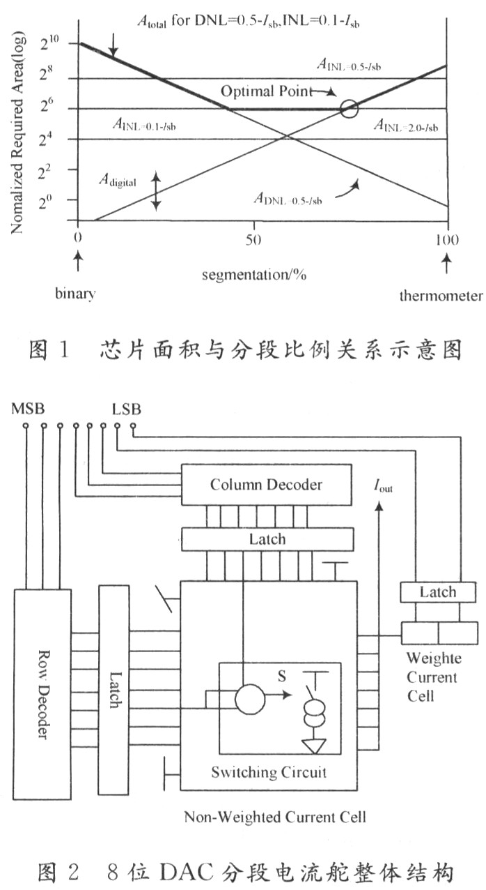
Figure 2 is an illustration of the basic structure of an 8-bit segmented current rudder. In the figure, the 6+2 segmentation structure is adopted, and the high 6-bit digital signals are converted into thermometer codes by Rows Decoders and Columns Decod-ers, respectively, and 26-1=63 unit currents are respectively controlled. The source constitutes an 8×8 current source matrix. The excess current source acts as a Dummy device, and the sum of the currents of the 63 unit current source and the low 2-bit binary weighted current source forms the current of the overall current source in the array.
2 Decoding Logic In current DAC designs, the current source unit, decoder, and glitch-free (noise) structure are important parts, and the performance of the DAC is determined by these parts. In order to improve dynamic linearity at high frequencies, a combinational logic decoding circuit composed of a transfer gate and a transistor is proposed here.
2.1 Transfer Gate Logic Since the NMOS transistor can be transferred through the logic variable 0, the PMOS transistor can be transferred through the logic variable 1, and the two MOSs are placed in parallel to form a complementary structure. Here, a transmission gate (TG) can be obtained, and for TG, the logical variables 0, 1 can be transmitted well. As we all know, the delay time between decoders is the main cause of glitch, and the logic designed with TG has better performance and less delay than all CMOS logic circuits. It has been verified that all two input logic gates can be composed of a transfer gate and an inverter. As an example, to implement NAND gate logic, all CMOS technologies require six transistors, but using a TG structure requires only five transistors. On the internal DAC chip, it has two signals and has a flip signal, so there is no need for an inverter, so the two transistors are reduced. The experimental results show that the chip area and power consumption are greatly reduced.
2.2 Logic Decoding Circuit In order to reduce power consumption and reduce delay, row and column decoding with minimum logic level should be designed. TG logic circuit is used to form 3~8-bit row and column decoder. Thus, the row decoder is obtained from the upper 3 bits and the column decoder is obtained from the intermediate 3 bit inputs. The row decoder circuit using TG is shown in Figure 3.
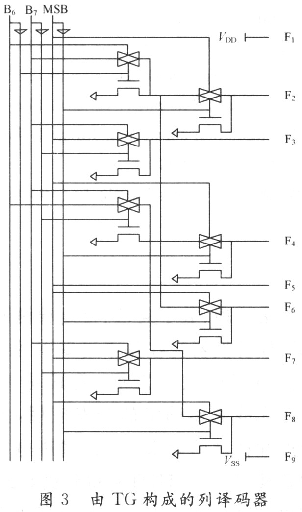
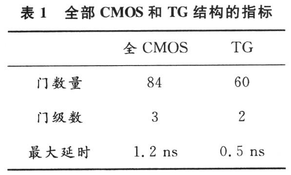
The row decoder structure is basically the same as the column decoder, but there is no power supply node. Another great benefit of using a TG logic decoder is that the number of transistors can be reduced. In static logic, the decoder of reference [9] consists of 84 transistors, but the row and column decoders consisting of TG structures have 30 transistors and the total number is 60. This means that the chip area may also be reduced. Fewer transistor levels also help reduce latency. On the other hand, the maximum number of logic gates using the TG structure can be reduced to 2 levels; the maximum gate level of a full CMOS structure without a transmission gate structure is 3, which fully demonstrates that the use of the TG structure is more advantageous for reducing delay and improving the operation. frequency. Table 1 gives the relevant parameter comparisons.
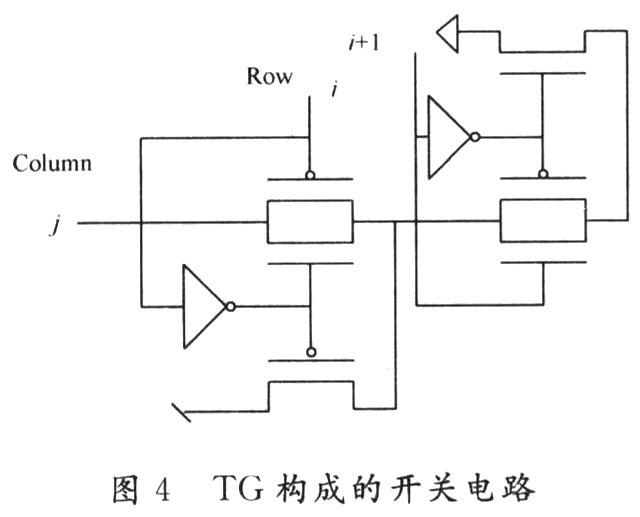
2.3 Working principle Decoding with row and column decoder, unit current source is turned on or off, there are three cases. The first is that the row and the next row are both "1", in which case the current source is selected regardless of whether the column control signal is "1". That is to say, the corresponding current source switching state is the on state. The second case is that the row control signal is "1", but the control signal of the next row is "0". At this time, whether the current source is selected or not depends on the column control signal. If the column control signal is "1", the current source is selected; if the column control signal is "0", the current source is not selected and is in an off state. In the third case, the control signals of the row and the next row are both "0", so the current source will not be selected regardless of the control signal of the column in which it is located, and is in the off state. The switching circuit composed of TG is shown in Fig. 4.
3 Current source circuit and glitch reduction circuit The current source circuit is an important part of the DAC. In order to reduce the glitch reaction, the circuit for reducing burrs will be described below.
3.1 Current Units Commonly used designs use complex structures that reduce circuit noise and reduce current sources. For example, differential circuits, bias circuits, reference currents, etc. require a large number of transistors. In this design, a simple current cell structure is used, and the current source uses a current source cell composed of two transistors. Compared to other chips, the area of ​​the circuit can be greatly reduced, as shown in Figure 5.
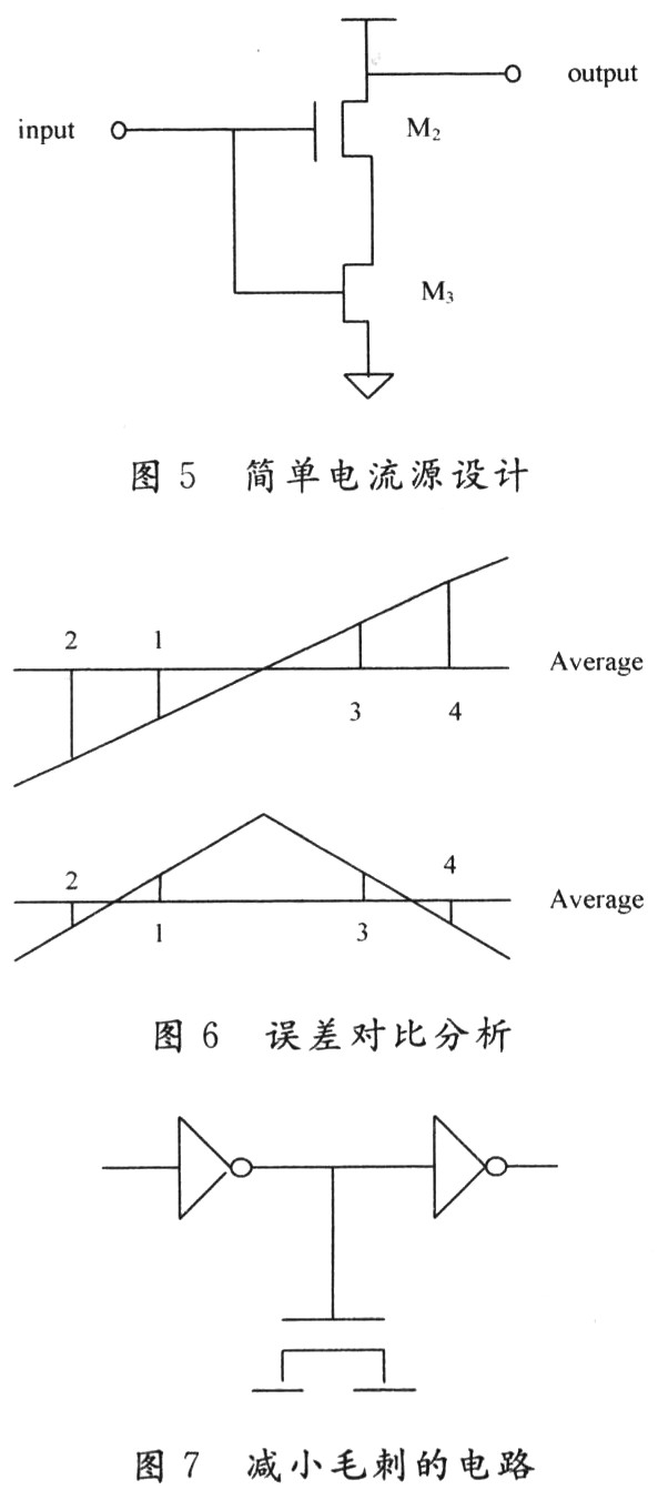
According to the comparison of the gradient error and the symmetry error shown in Fig. 6, the layout of the hierarchical symmetric switching sequence is adopted in the unit current source matrix, and the error is well reduced.
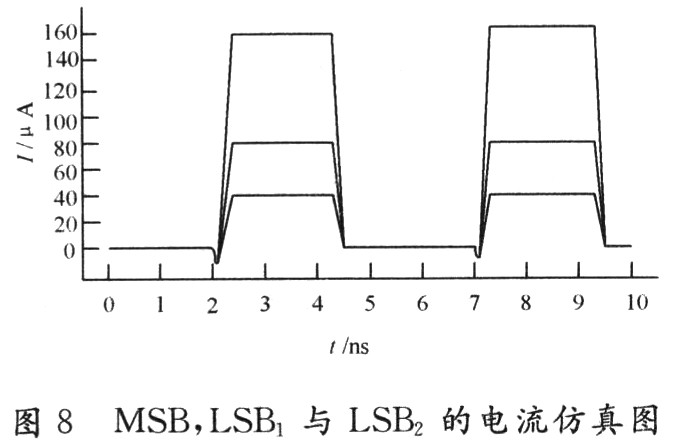
3.2 Circuit for reducing glitch In the basic current source unit, the output signal will be relatively stable. In this design the current source is controlled by the switching circuit output signal, but the output signal is not sufficiently accurate. Therefore, in order to compensate for this shortcoming while improving the SNR of the circuit, it is necessary to use a burr reduction circuit as shown in FIG.
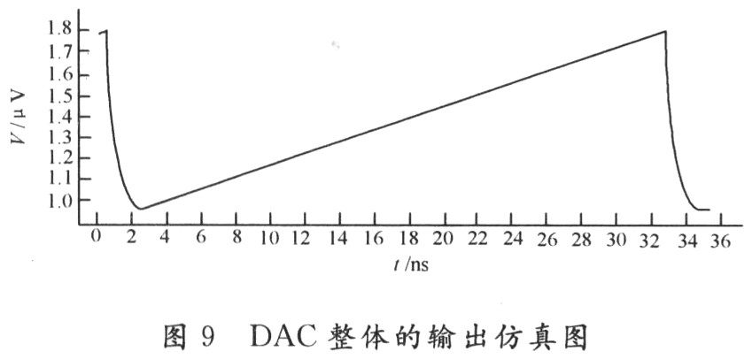
5 Experimental results The DAC designed in this paper is based on O. 25 μm CMOS technology, 8-bit high-speed DAC for high-definition video use, and the number of TG transistors and circuit stages can be significantly reduced, while using TG structure can also effectively reduce circuit delay time, and burrs are greatly reduced . The results show that this design can achieve 1.5 GHz sampling rate and 21 mW low power consumption.
The specific parameter indicators are shown in Table 2.
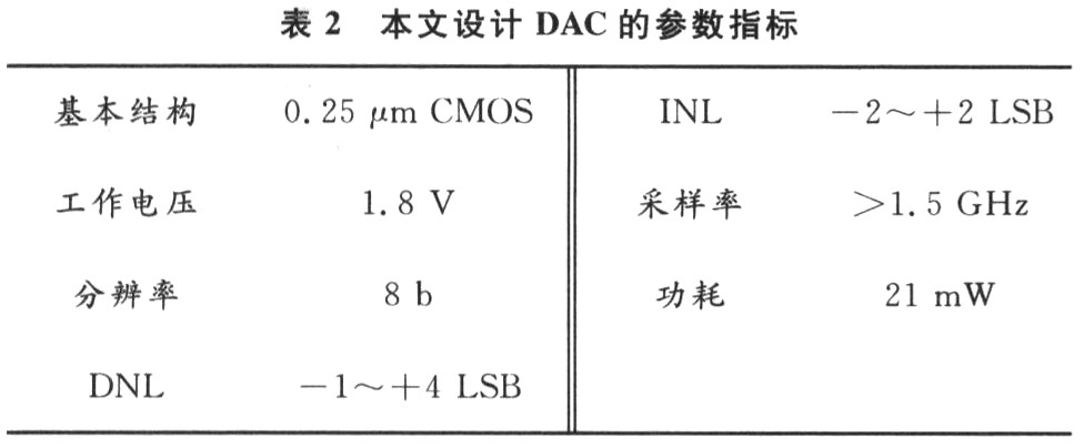
6 Conclusion This paper proposes a current source cell matrix based on a novel transmission gate (TG) structure, a decoding logic circuit, and a high-speed 8-bit CMOS current steering digital-to-analog converter (CS-DAC) for high definition video use. The decoding circuit of the current source unit matrix structure and the transmission gate structure can effectively reduce the interference signals such as burrs; the circuit designed by the TG structure can significantly reduce the number of transistors and the delay of the circuit; the DAC circuit design based on 0.25 μm CMOS technology It consumes only 21 mW and has a sampling rate of 1.5 GHz. The simulation results show that the integral linearity error (INL) of the circuit ranges from -2 to +2 LSB, and the differential linearity error (DNL) is -1 to +4 LSB.
Variable Frequency AC Power Supplies
The VFP series AC Power Supplies are high precision, high efficiency, low THD adjustable AC power supplies that converts the input mains power through AC→DC→AC conversion, and gives a pure sine wave AC output with adjustable voltage & frequency within a certain range. Also known as Variable Frequency AC Power Source.
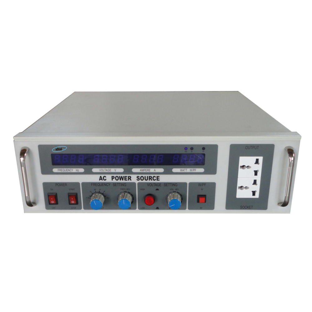
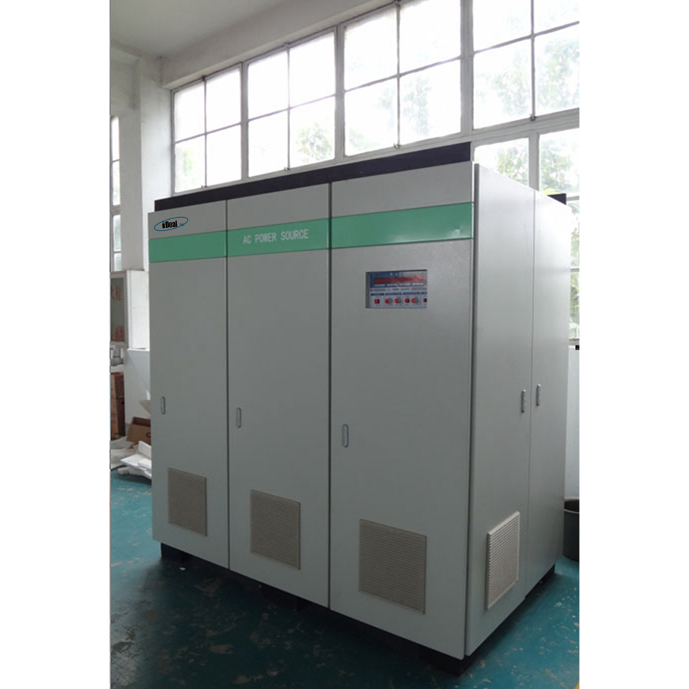
According to the difference in the number of output phases, it can be divided into single-phase and three-phase AC power supplies.
The output power of single-phase adjustable AC power supply ranges from 500VA to 200KVA, the output power of three-phase adjustable AC power supply ranges from 3KVA to 600KVA, the output voltage is divided into 0 ~ 150Vac, 150 ~ 300Vac, and the output frequency is adjustable from 45Hz to 70Hz with 50/60Hz fixed frequency output.
Through the friendly operation panel, you can read the output data such as output voltage, output current, output power, power factor, etc., providing accurate data records for your test, and can add RS485 interfaces as standard, following the MODBUS-RTU international communication protocol, which can realize remote control and operating status monitoring of the power supplies.
This series of adjustable AC Power Supplies have comprehensive protection functions, such as: over voltage, over current, over temperature and short circuit protections, which can protect the AC power supplies and DUT from damages. At present, it is mainly used for Various electrical appliance manufacturers conduct grid simulation tests on electrical appliances according to the voltage/frequency requirements of different countries. Imported electrical appliances are used for the domestic demand for variable voltage and frequency conversion, as well as various AC motors and AC transformers.
Variable Frequency AC Power Supplies, AC Variable Frequency Power Supplies, Variable Frequency AC Power Sources, Variable Frequency Power Supplies, Variable Frequency Power Sources
Yangzhou IdealTek Electronics Co., Ltd. , https://www.idealtekpower.com