The AD7656 has a maximum sampling rate of 4 LSBS INL and 250 kSPS per channel, and contains an internal 2.5V reference and reference buffer on-chip. The device consumes only 160mW of typical power and consumes 60% less power than the nearest competing bipolar input ADC.
The AD7656 contains a low noise, wideband track-and-hold amplifier (T/H) to handle signals up to 8MHz. The AD7656 also features high-speed parallel and serial interfaces that can interface with microprocessors (mcu) or digital signal processors (DSP). The AD7656 provides a daisy-chain connection in the serial interface mode to connect multiple ADCs to a serial interface.
AD7656 working principle:The AD7656 has an independent six-channel successive approximation (SAR) analog-to-digital converter. Conversion processing and data accuracy are controlled through the CONVST signal and an internal crystal oscillator. Three CONVST pins allow three ADCs to independently sample simultaneously. When 3 CONVST pins are connected together, simultaneous sampling of 6 channels is possible. The AD7656 has a high-speed parallel and serial interface that allows it to interface with Microprocessors and DSPs. When using the serial interface mode, the AD7656 has a daisy-chain feature that allows multiple ADCs to be connected to a serial interface. Since the design of the parallel interface connection is mainly used in the power relay protection products, the working principle of the parallel interface is described below.
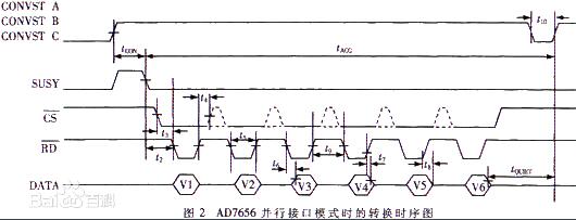
First, start the conversion with the MCU or DSP controlling the CONVST pin and keep this signal high. After the AD7656 starts the conversion signal, it will automatically output the BUSY signal. When the BUSY signal falls, it means that the conversion has been completed.
At this point, the AD7656 internal 6 registers have saved the converted data, and then read through the chip select CS and read RD signals sequentially read out the 6 channel AD conversion value. After reading the AD conversion value, change CONVST to a low level signal. Note that during design, it must be ensured that the CONVST pin stays high during AD conversion.
Application of AD7656:At present, relay protection products are constantly upgrading and changing design patterns. Initially due to various factors such as process and chips, the first-generation power relay products all use analog switches to match single-channel 16-bit ADC designs, such as AD976, AD574, and other AD converter products; later, the use of 16-bit AD7665 With the 14bit AD7685 with the second generation of relay protection products of analog switches, AD7665 and AD7865 still have very successful application cases in many current power relay protection products; with the update of technology and improvement of product technology, especially its With the technical features of ±10V bipolar multi-channel synchronous input, AD7656 is expected to become a new generation of power relay protection products.
Two, TMS320C6713 IntroductionThe TMS320C6713 DSP is a C6000 DSP chip introduced by TI in the United States in 1997. It is a 32-bit high-speed floating-point DSP with a maximum clock frequency of 300 MHz.
The main features of TMS320C6713 are:
(1) The architecture uses a very long instruction word (VLIW) structure. The single-instruction word length is 32 bits. There are 8 instructions in the instruction packet and the total word length is 256 bits. The functional units that execute the instructions are already allocated at compile time. When the program is running, a special instruction allocation module is used. Each 256-bit instruction packet can be allocated to 8 processing units at the same time, and 8 units can run simultaneously. Its maximum processing capacity can reach 2400 MIPS.
(2) The use of two-level buffering, 4KByte direct matching program buffer L1P, 4KByte matching data buffer L1D, 256KByteL2 additional matching memory. 32-bit external memory interface that seamlessly connects SRAM, EPROM, Flash, SBSRAM, and SDRAM.
(3) Abundant peripherals, including DMA, EDMA, support for transfer of data in the allowable address space without CPU involvement, expansion bus, host port and I/O port operations, etc., multi-channel buffered serial port, through which configuration Can communicate with various serial communication interfaces, two 32-bit general-purpose timers, etc.
Third, analog conversion circuit design 1, analog conversion circuit designSince the signal source collected by the integrated control computer does not match the input signal required by the AD7656, the front-end conditioning circuit of the signal source is adjusted. The design of the AD7656 front-end conditioning circuit mainly considers the following factors:
(1) Impedance matching. Because the signal source of the input signal is not necessarily low impedance, the input of the AD7656 is likely to divide the signal of the signal source, thereby affecting the accuracy of the acquisition conversion signal. An operational amplifier buffer is used to solve this problem in the AD7656 front-end input. Because the op amp buffer has a very high input impedance, it does not divide the signal source, and its low output impedance is suitable for driving the AD7656's input.
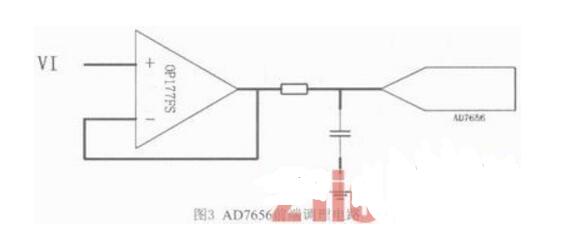
(2) Reduce the influence of capacitive loads. The AD7656's input has a capacitive load characteristic, which usually requires a resistor and capacitor to form an external compensation circuit that uses this circuit to add a capacitive load to the signal source.
AD7656 front-end conditioning circuit design shown in Figure 3. The AD7656 front-end conditioning circuit uses an OP177FS from Analog Devices, Inc., which has a low input offset voltage (25μV), maximum offset time offset of 0.1μV/°C, minimum open-loop gain of 12V/μV, and supply current of 2.0mA.
The AD7656 and TMS320C6713B interface circuits use a parallel interface design. In the circuit design, the “SER/PAR†pin of the AD7656 is set to the parallel interface mode, the “W/B†pin is set to the word mode, and the “H/SSEL†pin is set to the hardware start conversion mode. TMS320C6713B through the external memory interface (EMIF) bus access to the AD7656, start the AD7656 conversion, read the conversion result data, interface circuit structure shown in Figure 4.
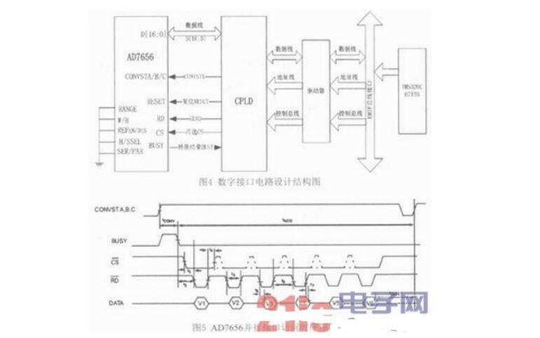
The TMS320C6713B decodes the AD7656's control logic through the CPLD to meet the logic requirements of the AD7656's access signals. The timing diagram of the AD7656 access is shown in Figure 5.
The AD7656 includes 6-channel ADC conversions for simultaneous conversion of 6-channel ADCs, reducing the sampling time of multiple ADC conversions. Controlling "CONVSTA" Simultaneously in CPLD Logical Design
The “CONVSTB†“CONVSTC†pin output effectively completes the simultaneous conversion of the 6-channel ADC channels.
According to Figure 5, the AD76565 starts ADC conversion with the rising edge of the “CONVSTA, B, C†signal. During the ADC conversion process, the “BUSY†signal is logic “highâ€. During ADC conversion, the ADC conversion clock is controlled by the internal clock. Generate, start ADC conversion after 3μs conversion from the rising edge of the “CONVSTA, B, C†signal. “BUSY†signal is logic “low†to indicate the end of ADC conversion. The TMS320C6713B completes reading the conversion results through the EMIF bus interface. The AD7656 chip conversion results are read and controlled by the "CS" chip select signal and the "RD" read signal. After the 6 channels are converted, the TMS320C6713B controls "CS" as valid and 6 "RD" read valid signals to complete the simulation. Input the reading of “V1†signal, “V2†signal, “V3†signal, “V4†signal, “V5†signal, and “V6†signal conversion result.
3, AD7656 design should pay attention to the problem3.1 Voltage Reference Circuit Design
Since the accuracy of the AD7656 conversion is highly dependent on the accuracy of the reference voltage reference, the voltage reference output voltage value is used to determine the full-scale input range of the data conversion system. Any error in the reference voltage reference can seriously affect the linearity of the ADC. No spurious dynamic range.
Due to the low accuracy of the voltage reference parameters integrated in the AD7656, a high-precision external voltage reference is generally used in ADC applications with a resolution greater than 12 bits. This design uses a high-precision external voltage reference AD780BR as the voltage reference for the AD7656 conversion. By comparing the two voltage reference parameters in Table 2, it can be seen that the external high-precision voltage reference has high accuracy, lower temperature coefficient, thermal hysteresis, and long-term drift.
Fourth, PCB design 1, the number of \ model divisionIn high-speed AD acquisition circuit design, achieving high precision and PCB design are inseparable, so in the PCB design process, according to the circuit to achieve the function can be simply divided into digital circuits and analog circuits in two parts, the digital area and simulation The area is divided to form an independent power source and ground for each area, which can effectively suppress the conduction of interference and the radiation of RF energy.
The AD7656 chip defines the analog and digital signals according to the area when the pins are defined, which is conducive to the digital and analog area division in the PCB design. When wiring, pay attention to the analog signal area, the analog signal line, and the digital signal area to the digital signal line. Do not route digital and analog signal lines in parallel.
In this system, a potential reference point is used analogically and digitally, so the analog ground and the digital ground use a single point common ground. The common location is as close as possible to the AD7656.
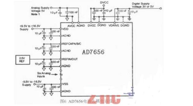
2, power supply decoupling designBecause there are multiple power pins on the AD7656, decoupling capacitors are required on each power pin. The design of the decoupling capacitor uses parallel 100nF and 10μF capacitors. A small equivalent series inductance (ESL) ceramic dielectric capacitor may be used for capacitor selection. The decoupling capacitor design of the AD7656 is shown in Figure 6.
TI offers a good C/C++ compiler that supports C/C++ language design during the open process of the TMS320C6713B software. And provides a good library function (DSPLIB), support TMS320C6713B math operations and vector operations.
The acquisition software design adopts a modular design, mainly including the initialization function, the AD7656 conversion start function and the read function of the AD7656 conversion result.
The initialization function implements the configuration of the TMS320C6713B system clock, the EMIF bus clock configuration, and the EMIF bus interface access timing. Through the initialization function configuration, the CS (chip select) RD read signal relative timing relationship is configured to meet the AD7656 access timing relationship.
The AD7656 conversion start function implements the AD conversion of the AD7656. This function controls the AD7656 conversion start signal CONVSTA, B, and C to be active and synchronizes 6 AD conversions.
The AD7656 conversion end identifier query function performs a BUSY query on the AD7656 conversion status identification signal to determine whether the internal ADC conversion of the AD7656 has ended.
The AD7656 conversion result read function reads the AD conversion result after the file is queried to the end of the AD conversion. This function reads 6 AD synchronous conversion results through 6 consecutive read operations. The process of AD acquisition software is shown in Figure 7.

For high-precision, multi-channel signal monitoring and real-time acquisition, this design uses the combination of AD7656 and TMS320C6713B as a control system working status real-time monitoring and fault detection system program. This design interface circuit is simple in design, high accuracy and high speed. The acquisition of multiple signals can be completed at the same time. The joint test of the system proves that the system fully meets the requirements of a control system for the monitoring of the working status and the acquisition accuracy and real-time performance of the fault detection signal.
Biotept main gear motors are micro DC and AC gear motors and right-angle gear motors
1. Motor & Gear head Dimensions : 60mm, 70mm, 80mm, 90mm, 104mm
2. Power: 6W, 15W, 30W, 40W, 60W, 90W, 120W, 180W, 200W, 250W
3. Voltage:
AC: Single/three phase, 110V 220V 380V
DC:12V 24V 60V 90V 110V 220V ..
4. Output Speed :
AC:500-3.0 r/min
DC 16RPM -1000RPM
5.Output Torque :
AC: 0.13-39.2 N.m
DC: 0.04-40 N.M
You can contact us for more details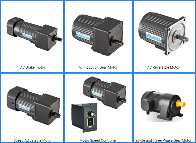
Brake Motor,Electric Motor Brake,Brek Pad Motor,3 Phase Brake Motor
Ningbo Biote Mechanical Electrical Co.,Ltd , https://www.biotept.com