Signal integrity has always been a concern for analog engineers, but as serial data link transmission rates move toward the GHz class, digital hardware designers must now also focus on this important issue.
Currently, high-speed serial links between chips have been widely used to increase the throughput of narrower bus bandwidths. Some of the latest DSPs and processors have begun to adopt Serial RapidIO. For many hardware designers, the use of bus speeds above 300MHz for inter-chip communication is a new challenge, while high-quality data links that design GHz-level data rates are More care and understanding is required to ensure that board design and noise do not compromise performance.
This article explores some of the Signal Integrity (SI) issues and considerations that designers may face, highlights the issues they face, and makes some recommendations. To illustrate how to apply these principles, this article describes a 16-port serial RapidIO switch.
Precautions
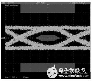
Signal quality is very important. In serial RapidIO, it is quantified by the size and shape of the receiving eye. The receiving eye is an infinitely continuous trajectory in which the waveform continues with the previous trajectory (Figure 1). If noise or other random signals are absorbed in the signal path, it will cause signal jitter and contraction of the receiving eye, resulting in degradation of signal quality.

Figure 1 contains a range of trajectories for receiving eye diagrams

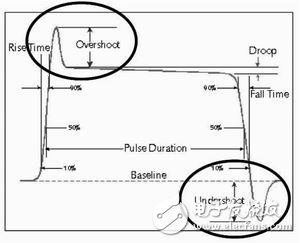
Figure 2 Typical characteristics of pulse overshoot and undershoot
Most of the best practices for lower frequency board designs need to be modified at frequencies above 300MHz. FR4 materials may also be successfully used as base materials, but at higher frequencies, the dielectric constant and loss factor of the material need to be reconsidered in impedance calculation and trajectory modeling. The design of via vias has also become important because unused tubular lengths exhibit impedance that is not matched to thicker boards and backplanes. Please post a design simulation to verify performance and pay attention to paths where signal integrity is less than ideal, while pointing out the crosstalk area.
Reflections caused by impedance mismatch can cause overshoot, undershoot, and ringing of the signal line forming the differential pair (Figure 2), as well as shrinking of the receiving eye.
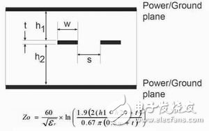
Improper wiring layers, improper design of jump paths, and improper connector selection can also cause unmatched artifacts in the signal. The impedance requirement for the serial RapidIO interface is 100Ω differential. The proposed construction method is to use edge-coupled differential strip lines (or coplanar strip lines), which is shown in Figure 3. The equations for single-ended and differential impedance are also provided. The routing between different layers should be minimized when routing. In addition to BGA pads, typically up to two paths are allowed per path.
The return current path is defined as the path that passes when the current returns to the starting point - through the formation, power plane, other signal paths, and through the IC. The integrity of the return path can be evaluated by plotting a tracking current from the driver through the signal conductor to the receiver loop - the smaller the loop area, the lower the self-inductance produced.
The following design rules apply to all return paths.
- Do not transmit impedance-constrained signals through the cracks in the reference layer.
- Do not transmit signals on the reference layer.
- Changing the signal layer does not force the return path to make changes to the reference layer. If the reference layer must be changed, change from one VSS reference layer to another VSS reference layer and place a path connecting the two layers as close as possible to the signal path. This rule also applies to reference layer changes from one VCC layer to another.
- Do not send signals through the reverse side of the via or the back pad of the slot.
If the distance between paths belonging to different signal groups is too close, crosstalk will result. In the serial communication link, the result is that the receiving eye is closed due to jitter. This may also be due to improper implementation of the path curve, some of the signals use short paths (the jump of the curve), while the main signal uses long paths, causing problems with path length matching. In very dense designs, crosstalk can be solved by using a protection path in which the lines arrive parallel to the signal path and to the reference.
Clock generation and buffering can cause noise unless you pay attention to some details, such as decoupling and the manufacturer's layout guidelines, to ensure the highest quality output. The impedance of the path must be tightly controlled to avoid unwanted reflections. The complexity of the design and the introduction of routing gaps in the power and ground planes can also cause high noise levels in the clock generator.
If there is not enough copper wire for the instantaneous current or the decoupling capacitor is not in the proper position, it will cause power distribution. Single-ended parallel buses generate transient currents in the power plane and ground plane, creating noise.
Interconnects consisting of cables and connectors designed for high frequency and G-class applications should be used in high bit rate systems. Using the wrong type or improperly matching the cable and connector will reduce the quality of the signal and will not recover.
When selecting components, you must choose a suitable manufacturer whose components should be designed to solve high-speed design problems. The device must provide sufficient power consumption and properly placed and separated ground connections to avoid instability in the chip core supply, avoid noise, and supplement with an effective decoupling strategy. For controlling noise, the separation between the core logic power supply and the ground and the I/O power supply and the ground is also critical. Proper equipment and excellent design will help meet high speed requirements and enable designers to effectively address signal integrity issues.

Figure 3 suggests the edge-coupled differential stripline configuration, which shows the equation for single-ended impedance Z0 and differential impedance Zdiff.

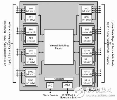
Figure 4 Structure of the Tsi568A Serial RapidIO Switch Interface
16-port serial switch
Tundra Semiconductor's Tsi568A is a standards-based, high-performance, 16-port serial RapidIO switch. RapidIO is a peer-to-peer packet-switched interconnect protocol designed to meet the needs of today's and tomorrow's embedded applications. It provides high-speed strings between data layer processing elements in processors, bridges, remote memory or embedded applications. Line interconnection. Figure 4 shows the main components of the device.
The most typical applications are wireless embedded communications (Node B, Radio Network Controller, and Media Gateway).
Designed to achieve the highest signal integrity standards, the Tsi568A includes features such as a low noise logic core and a high performance flip chip BGA package.
Conclusion
As long as you follow some basic but important design principles, you can use high-frequency interconnects (such as RapidIO) in your system without the traditional signal integrity problems. Good signal integrity can be easily achieved if the path and signal path are minimized, shielded by the ground plane, or physically isolated from each other, and impedance mismatches can be carefully avoided.
Pmic Led Drivers,Ic Pmic - Led Driver,Pmic Led Driver Ic Chip,Pmic Led Drivers Ic
Shenzhen Kaixuanye Technology Co., Ltd. , https://www.iconlinekxys.com