The phase-locked loop is an automatic phase control circuit for the purpose of eliminating frequency error. It can complete the automatic control closed-loop system of phase synchronization of two electrical signals, referred to as PLL. Since the phase-locked loop has the characteristics of no frequency difference after locking, it is widely used in the technical fields of broadcast communication, frequency synthesis, automatic control, and clock synchronization.
Motor speed measurement with phase-locked loop CD4046----integrated phase-locked loop CD4046In the past, phase-locked loops were mostly composed of discrete components and analog circuits. Nowadays, phase-locked loops of integrated circuits are often used. Because integrated phase-locked loops have excellent performance, low cost, and convenient use, they are widely used. It should be pointed out that the integrated phase-locked loop often does not contain a loop filter. Therefore, different R and C components must be externally connected to form a loop filter, so that the phase-locked loop has different performances to be applied to different occasions. The integrated phase-locked loop CD4046 is one of them.
Features of CD4046The phase-locked loop CD4046 is a general-purpose CMOS digital phase-locked loop [2, 3]. The maximum operating frequency is about 1MHz. The power supply voltage range is wide (3~8V), the input impedance is high (about 100MΩ), and the dynamic power consumption is extremely low. The power consumption is only 600μW at the center frequency f0 of 10kHz, which is a micro power device.
Pin function of CD4046The CD4046 uses a 16-pin dual in-line type with pinouts as shown below.
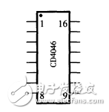
The function of each pin is as follows:
Pinout of CD4046
1 pin: Phase output terminal, the loop is high when the loop is locked, and the loop is low when the loop is lost.
2 feet: the output of the phase detector I.
3 feet: Compare signal input.
4 feet: voltage controlled oscillator output.
5 feet: Disabled, disabled at high level, allowing the voltage controlled oscillator to work when low.
6, 7 feet: external oscillating capacitor.
8, 16 feet: the negative and positive ends of the power supply.
9 feet: the control end of the voltage controlled oscillator.
Pin 10: Demodulation output for FM demodulation.
11, 12 feet: external oscillating resistor.
13 feet: the output of the phase detector II.
14 feet: signal input.
Pin 15: Internal independent Zener regulator tube negative.
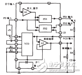
Internal structure and working principle of CD4046The internal electrical block diagram of CD4046 is shown in Figure 3. It mainly consists of a voltage controlled oscillator (VCO), a source follower (A2), a voltage regulator, a linear amplification and shaping circuit (A1), and two phase detectors (I, II).
The phase detector I adopts an exclusive OR gate structure. When the level states of the two input signals Ui and Uo are different (ie, one high level and one low level), the output signal UΨ is high level; otherwise, Ui When the Uo level is the same (that is, both are high, or both are low), the UΨ output is low. When the phase difference Δφ of Ui and Uo changes between 0 and 80°, the pulse width of UΨ will also change, that is, the duty ratio also changes. For phase detector I, it requires Ui, Uo to have a 50% duty cycle (ie, square wave), so that the lock range is maximized.
Phase Detector II is a digital memory phase detector that is triggered by the rising edge of the signal. It does not require a high duty cycle on the input signal, allowing an input of an asymmetric waveform. It has a wide range of capture frequencies and does not lock the harmonics of the input signal. The two phase detectors are output by pins 2 and 13, respectively, and can be selected as needed. The phase detector II has another output (pin 1) that outputs an output lock signal (phase pulse) that can be used as an indication of the locked state of the phase locked loop. When the lock is reached, a 0° phase shift is maintained between the two input signals of phase detector II.
Since the input signal Ui (input from pin 14) is generally small, it does not meet the requirements of the above two digital phase detectors for the input signal level, and the waveform is irregular, so the input signal is first amplified and shaped by the circuit A1. Its level and waveform meet the requirements of the phase detector (I, II).
The loop filter uses an external RC network (R3, R4, R2) whose output control voltage is connected to the input of the voltage controlled oscillator (VCO) (9-pin).
The CD4046 phase-locked loop uses a cross-charge-discharge type voltage-controlled oscillator. Therefore, an external capacitor C1 and a resistor R1 are used as charge and discharge elements between pins 6 and 7. An external resistor R2 is also required when the PLL requires a frequency width of the tracked input signal. Since the VCO is a current-controlled oscillator, the charging current of the timing capacitor C1 is proportional to the control voltage input from the 9-pin, so that the oscillation frequency of the VCO is also proportional to the control voltage. When the VCO control voltage is 0, its output frequency is the lowest; when the input control voltage is equal to the power supply voltage VDD, the output frequency linearly increases to the highest output frequency. The range of the VCO oscillation frequency is determined by R1, R2, and C1. Since its charging and discharging are performed by the same capacitor C1, its output waveform is a symmetrical square wave. Generally, the maximum frequency of CD4046 is 1.2MHz (VDD=15V). If VDD is 15V, fmax should be reduced.
When the CD4046 is used for demodulation of the FM wave, the control voltage output from the loop filter is passed through the source follower (A2) to pin 10 to obtain a demodulated signal of the FM. Note that the load resistor R5 must be connected between pin 10 and ground.
The CD4046 also has a voltage regulator consisting of a Zener diode (regulated voltage Uz = 5~8V). When the CD4046 matches the TTL circuit, the Zener can be used as an auxiliary power source.
In summary, the CD4046 works as follows: After the input signal Ui is input from the 14-pin, it is amplified and shaped by the amplifier A1 and applied to the input terminals of the phase detectors I and II. The switch K is switched to the 2nd pin. The phase comparator I compares the phase comparison signal Uo input from the 3 pin with the input signal Ui, and the error voltage U 输出 outputted from the phase detector I reflects the phase difference between the two; U 滤波 is filtered by R3, R4 and C2 A control voltage Ud is applied to the input terminal 9 of the VCO to adjust the oscillation frequency f2 of the VCO so that f2 quickly approaches the input signal frequency f1; the output of the VCO is then passed through the frequency divider and then enters the phase detector I (determining the frequency division as needed) The presence or absence of the device continues to phase comparison with Ui, and finally makes f2=f1, the phase difference between the two is a certain value, and phase locking is realized. If the switch K is set to 13 feet, the phase detector II operates, and the process is the same as described above.
Internal electrical schematic of CD4046
Keystone Jack,cat6 keystone,cat6 jack,cat6 wall jack
NINGBO UONICORE ELECTRONICS CO., LTD , https://www.uniconmelectronics.com