1 audio analog chip TLC320AD50C
TI's TLC320AD50C uses oversampling ΣΔ technology. There is an interpolation filter in front of the DAC and a sampling filter after the ADC. This structure allows the system to receive and send simultaneously. And TLC320AD50C can achieve high resolution, low speed signal, high sampling rate (up to 22.5kb / s) AD / DA conversion. It consists of a pair of 16-bit synchronous serial conversion channels and can be directly connected to the DSP for communication.
The characteristics of TLC320AD50C are as follows:
(1) The ADC in the device is 64 times oversampling, and the DAC is 256 times oversampling (internal);
(2) With built-in anti-aliasing filter and sinx / x compensation;
(3) It can be configured as a master or slave mode, a serial interface can support 3 slave devices to communicate with DSP. ?
The options and circuit configuration in the TLC320AD50C can be programmed through the serial port. The specific programmable items are: reset, power down, communication protocol, serial clock rate, signal sampling rate, gain control, test mode, etc.
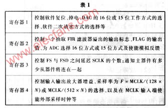
TLC320AD50C has 7 control registers, of which the main 4 register functions are shown in Table 1. Since register 4 can modify the sampling frequency, it may be modified frequently, and it is often involved in secondary communication.
2 TLC320AD50C and TMS320C30DSP chip connection
TMS320C30 is a typical one of TI's floating-point arithmetic DSP chips. Its main clock reaches 40MHz. It uses a 32-bit floating-point arithmetic processor, which can realize high-speed floating-point arithmetic such as adaptive signal processing and signal conversion. Cost-effective products.
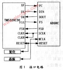
This article uses the interface circuit of TLC320AD50C and TMS320C30 to complete the data collection and TLC320AD50C register reading and writing process. The interface circuit of TMS320C30 and TLC320AD50C is shown in Figure 1.
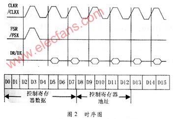
The main pins connected to the chip have a reset signal RESET; synchronization signals: FS, FSD (delayed frame signal) on AD50C, FSX (frame transmission signal), FSR (frame reception signal) on TMS320C30; data read and write signals: DIN, DOUT, DX, DR; clock signal: SCLK, MCLK, CLKX; secondary communication request: FC on AD50C, XF on C30. Under the action of the clock signal, C30's frame signal (FSX, FSR) and data transmission (DR, DX) timing diagram is shown in Figure 2. The off-chip reset circuit provides power-on reset, and the crystal oscillator circuit can provide the main clock frequency above 10MHz, and the data sampling frequency and other clock signals are all allocated by this frequency. There are two communication formats between C30 and AD50C, namely the main serial communication format and the secondary serial communication format. The former is used to receive and send conversion signals, while the latter only conducts secondary communication when requested. In the main serial communication format, there are two data transmission modes: 16 bits and 15 + 1 bits, which can be set through the control register, and 15 + 1 bits in the case of disregard. Using 15 + 1 bit transfer mode, the lowest bit D0 is a non-data bit, the D0 bit of the input DAC data is the secondary communication request bit, and the D0 bit of the output ADC data is the status bit of the M / S pin.
Secondary communication is only generated when a request is sent. When the first communication adopts the 15 + 1 bit mode, D0 can be used for the second communication request. When the first communication adopts the 16 bit mode, the FC pin must be used to generate a secondary signal. Communication request. The secondary communication data format is shown in Figure 2, where D7 ~ D0 are control register data, D12 ~ D8 are control register addresses, D13 = 1 is to read control register data, and D13 = 0 is to write data to the control register. Through the secondary communication, the TLC320AD50C can be initialized and the TLC320AD50C internal control register can be modified.
3 Data acquisition circuit and communication software implementation
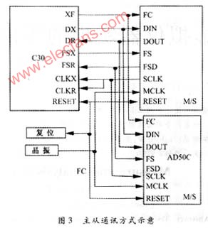
The FSD of the master AD50C is connected to the FS end of the slave chip, see Figure 3.
First set the relevant registers. If an analog signal with a sampling rate of 8 kHz is required and the clock input frequency to the TMS320C30 device is 30 MHz, the following values ​​should be loaded into the C30 serial port and timer.
The specific communication process is as follows: AD50C data input and output are connected to the C30 data receiving pin. The frame frequency signal sent by the AD50C is synchronized with the C30 through the FS pin. FSD is a synchronous delay signal. It is mainly used to expand the master and slave devices. S can control the master-slave mode of AD50C. The clock and synchronization signal pins in C30 can be set as external input by software. In this way, data transmission / reception, frame synchronization, clock signals are generated by AD50C, the main clock (MCLK) signal is provided by crystal oscillator, and FC and XF terminals are used as secondary communication requests. Assuming that the data transmission format is 16 bits, the secondary communication request is issued when the FC is high.
The flow chart of the program is shown in Figure 4.
4 Conclusion
This article introduces two typical chip connections, so that the data reading and writing of the register during the data collection process is well achieved, and it is also well applied in practice.
TI's TLC320AD50C uses oversampling ΣΔ technology. There is an interpolation filter in front of the DAC and a sampling filter after the ADC. This structure allows the system to receive and send simultaneously. And TLC320AD50C can achieve high resolution, low speed signal, high sampling rate (up to 22.5kb / s) AD / DA conversion. It consists of a pair of 16-bit synchronous serial conversion channels and can be directly connected to the DSP for communication.
The characteristics of TLC320AD50C are as follows:
(1) The ADC in the device is 64 times oversampling, and the DAC is 256 times oversampling (internal);
(2) With built-in anti-aliasing filter and sinx / x compensation;
(3) It can be configured as a master or slave mode, a serial interface can support 3 slave devices to communicate with DSP. ?
The options and circuit configuration in the TLC320AD50C can be programmed through the serial port. The specific programmable items are: reset, power down, communication protocol, serial clock rate, signal sampling rate, gain control, test mode, etc.
TLC320AD50C has 7 control registers, of which the main 4 register functions are shown in Table 1. Since register 4 can modify the sampling frequency, it may be modified frequently, and it is often involved in secondary communication.
2 TLC320AD50C and TMS320C30DSP chip connection
TMS320C30 is a typical one of TI's floating-point arithmetic DSP chips. Its main clock reaches 40MHz. It uses a 32-bit floating-point arithmetic processor, which can realize high-speed floating-point arithmetic such as adaptive signal processing and signal conversion. Cost-effective products.
This article uses the interface circuit of TLC320AD50C and TMS320C30 to complete the data collection and TLC320AD50C register reading and writing process. The interface circuit of TMS320C30 and TLC320AD50C is shown in Figure 1.
The main pins connected to the chip have a reset signal RESET; synchronization signals: FS, FSD (delayed frame signal) on AD50C, FSX (frame transmission signal), FSR (frame reception signal) on TMS320C30; data read and write signals: DIN, DOUT, DX, DR; clock signal: SCLK, MCLK, CLKX; secondary communication request: FC on AD50C, XF on C30. Under the action of the clock signal, C30's frame signal (FSX, FSR) and data transmission (DR, DX) timing diagram is shown in Figure 2. The off-chip reset circuit provides power-on reset, and the crystal oscillator circuit can provide the main clock frequency above 10MHz, and the data sampling frequency and other clock signals are all allocated by this frequency. There are two communication formats between C30 and AD50C, namely the main serial communication format and the secondary serial communication format. The former is used to receive and send conversion signals, while the latter only conducts secondary communication when requested. In the main serial communication format, there are two data transmission modes: 16 bits and 15 + 1 bits, which can be set through the control register, and 15 + 1 bits in the case of disregard. Using 15 + 1 bit transfer mode, the lowest bit D0 is a non-data bit, the D0 bit of the input DAC data is the secondary communication request bit, and the D0 bit of the output ADC data is the status bit of the M / S pin.
Secondary communication is only generated when a request is sent. When the first communication adopts the 15 + 1 bit mode, D0 can be used for the second communication request. When the first communication adopts the 16 bit mode, the FC pin must be used to generate a secondary signal. Communication request. The secondary communication data format is shown in Figure 2, where D7 ~ D0 are control register data, D12 ~ D8 are control register addresses, D13 = 1 is to read control register data, and D13 = 0 is to write data to the control register. Through the secondary communication, the TLC320AD50C can be initialized and the TLC320AD50C internal control register can be modified.
3 Data acquisition circuit and communication software implementation
The FSD of the master AD50C is connected to the FS end of the slave chip, see Figure 3.
First set the relevant registers. If an analog signal with a sampling rate of 8 kHz is required and the clock input frequency to the TMS320C30 device is 30 MHz, the following values ​​should be loaded into the C30 serial port and timer.
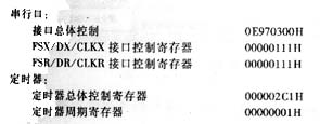
The specific communication process is as follows: AD50C data input and output are connected to the C30 data receiving pin. The frame frequency signal sent by the AD50C is synchronized with the C30 through the FS pin. FSD is a synchronous delay signal. It is mainly used to expand the master and slave devices. S can control the master-slave mode of AD50C. The clock and synchronization signal pins in C30 can be set as external input by software. In this way, data transmission / reception, frame synchronization, clock signals are generated by AD50C, the main clock (MCLK) signal is provided by crystal oscillator, and FC and XF terminals are used as secondary communication requests. Assuming that the data transmission format is 16 bits, the secondary communication request is issued when the FC is high.
The flow chart of the program is shown in Figure 4.

4 Conclusion
This article introduces two typical chip connections, so that the data reading and writing of the register during the data collection process is well achieved, and it is also well applied in practice.
Ncm Battery,Lithium-Ion Battery With Ncm Material,18650-2800Mah Battery,Nicomn Lithium Battery
Henan Xintaihang Power Source Co.,Ltd , https://www.taihangbattery.com