The normal operation of electronic equipment requires a stable and stable DC power supply. Most of the external power supply is now AC, usually obtained by thermal power generation, hydropower generation, nuclear power generation and wind power generation. The resulting AC power is converted to the DC power supplies of the various types of electronics required by the DC regulator for use. When the grid or load changes, the DC regulated power supply maintains a stable output voltage with a small ripple. Since the development of regulated power supply for more than half a century, the technology has become increasingly mature. In the past 20 years, the integrated switching power supply has developed in two directions; the first direction is the integration of the control circuit of the switching power supply.
The second direction is to realize the monolithic integration of medium and small power switching power supplies. There are many types of regulated power supply products on the market, and most of them meet the characteristics of high efficiency, stable output and high reliability. Most use high frequency transformers, which are relatively expensive. The DC voltage regulator adopts Sepic and Buck circuits as the main circuit, and the auxiliary power supply adopts high-frequency transformers, making full use of modern power electronics technology to output stable DC voltage when inputting AC power in a wide range under the premise of satisfying reliability and stability. And the cost is relatively low, easy to debug and repair.
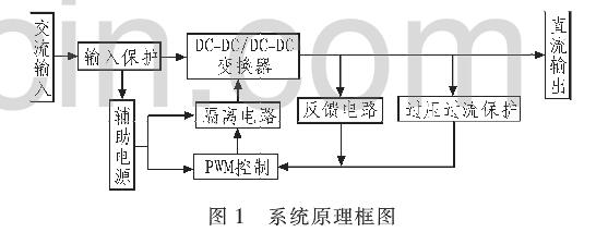
The high-voltage DC generated by the rectification and filtering of the AC input voltage through the input protection circuit serves as the input voltage of the auxiliary power supply, thereby providing the working voltage of the chip; and the input voltage of the DC-DC/DC-DC converter, DC-DC/DC The DC converter is a device for performing power conversion, and is a core port 2 of the switching power supply. The output voltage of the DC-DC/DC-DC converter is sampled by a feedback circuit to compare with a set reference voltage, and the PWM duty ratio is adjusted. The output voltage is then adjusted to keep it stable. The output has an overvoltage and overcurrent protection circuit. When the voltage and current are too large, the PWM signal is turned off and there is no voltage output. The system block diagram is shown in Figure 1.
The input protection part mainly includes a varistor RV, a thermistor RT, a fuse, a filter coil L0, and a rectifier bridge and a filter capacitor C16. The varistor RV is used for overvoltage protection of the AC input, that is, surge absorption. The filter coil LO and the capacitor CO constitute EMI and filter out noise interference. When selecting a rectifier bridge device, consider that it can withstand sufficient reverse withstand voltage, and the inrush current is greater than 7~10 times of the rated rectified current. The thermistor RT is a negative temperature characteristic (NTC) resistor that limits the peak value of the charging current of C16 at startup. After the startup, the resistance of the resistor will be reduced to a small value, and the power consumed is basically negligible. Its circuit diagram is shown in Figure 2.
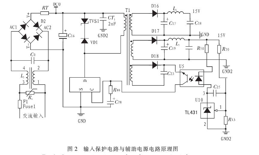
When the designed Sepic DC regulator is working properly, it needs to provide two independent power supplies for the PWM control chip and the isolated drive. The auxiliary power supply adopts single-ended flyback circuit, and its control chip adopts PI company's TOPSwitch II series. The device integrates control functions, protection functions and 700V power switch MOSFETs. It has leading edge blanking design and automatic Re-start function, low electromagnetic interference (EMI), voltage-type control mode and cycle-by-cycle peak current limit. Considering that the PWM control chip and the isolation chip work at a lower power, the TOP221Y is used, and the power output is 7W under a wide range of input power voltages, which is sufficient for the requirements. The circuit diagram of the auxiliary power supply is shown in Figure 2, and the principle analysis is as follows:
The AC power is rectified by full bridge, and the capacitor filter is used as the power supply for the auxiliary power supply. CT1 is used to filter out interference. During the turn-off of the MOSFET, due to the leakage inductance of the high-frequency transformer, the leakage voltage is very high. To protect the transformer from damage, the fast recovery diode VD1 and the transient suppressor TVS are selected to form a clamp circuit for absorbing leakage. The sense voltage and protection principle are analyzed as follows: When the MOSFET is turned on, the voltage across VD1 is up and down, VD1 is off, and the clamp circuit is not working. When the MOSFET is turned off, the voltage across VD1 changes due to leakage inductance. In order to go up and down, VD1 is turned on, the clamp protection circuit works, and the voltage is limited. The feedback loop mainly consists of a photocoupler PC817 and a three-terminal regulator TL431 and a number of resistors and capacitors. The linear optical coupler PC817 has a current transfer ratio (CTR) ranging from 80% to 160%, which can better satisfy the feedback loop. Claim. The resistor Rao.R3 is divided into TL431 reference voltage. By setting the resistance of R3O and R4, the regulated value of the required output voltage can be obtained. As the frequency compensation capacitor of TL431, GZ can improve the transient frequency response of TL431. RSO is the LED current limiting resistor of PC817, which acts as a current limiting protection. The principle of the feedback loop to achieve output voltage regulation is as follows: When the output voltage fluctuates, the sampling voltage U10 obtained by dividing the voltage of R3O and R43 changes the output voltage UK of the TL431, thereby controlling the illuminance of the light-emitting diode (LED) of the PC817, causing the light-sensitive The triode emitter current is proportionally changed. Finally, the TOP221Y control terminal current change is used to adjust the duty cycle to the opposite change, to achieve the purpose of stabilizing the output voltage, and to provide a stable auxiliary power supply for the circuit.
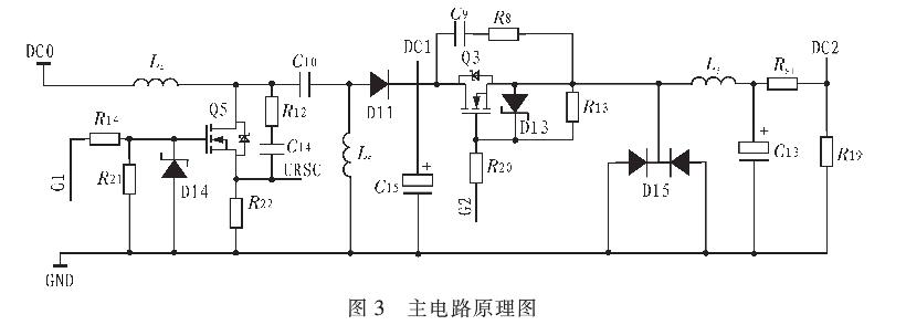
4, the design of the main circuit moduleThe DC chopper circuit functions to change one DC power to another fixed voltage or adjustable voltage. Applications can be divided into two categories: one is to output a variable DC voltage; the other is to output a constant DC voltage when the power supply voltage or negative cut is changed. The designed power supply belongs to the latter, and its schematic diagram is shown in Figure 3. The high-voltage DC voltage DCO stabilizes the varying voltage DCO (183~425 V) around DC1 through the characteristics of the liftable voltage of the Sepic circuit, and acts as a Buck circuit. Input voltage, set the appropriate duty cycle to get the output voltage DC2 (24 V), chopper circuit uses closed-loop feedback control, the AC supply voltage or output load resistance changes, the regulator output voltage can remain stable. Both DC-DC conversions include input and output filtering, and the voltage ripple is smaller. Both ends of the power tube drain and source adopt a RC absorption circuit composed of non-inductive resistors and capacitors, which absorb the peak voltage of the switch tube and protect the power tube.
The PWM control circuit is closely related to the performance of the DC-DC/DC-DC converter, so the design of the PWM control circuit is particularly important. The PWM control chip is selected from Silicon General's SG3525, which has an undervoltage lockout circuit, a soft start circuit, a reference voltage source, an error amplifier, an output current limit, and a shutdown circuit. The totem pole type is provided. Output stage, oscillator and adjustable deadband are widely used in the design of switching power supplies. The SG3525 peripheral circuit is shown in Figure 4, and the analysis is as follows.
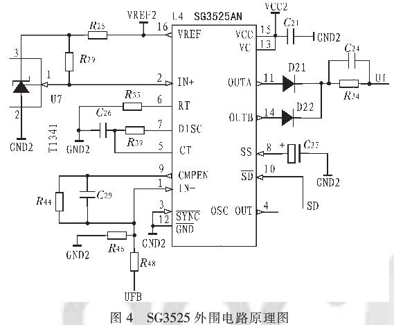
The reference voltage of TI431 manufactured by Texas Instruments (TI) was selected as the 2-pin reference voltage, and the output PWM control signal has high stability. R4 and C2 form the feedback compensation network between pins 1 and 9. The feedback voltage UFB is applied to pin 1 to compare with the reference voltage U7 of pin 2 to adjust the duty ratio. 14 and 11 feet of two outputs and one output, which makes the converter duty cycle adjustable range doubled. The CU is an accelerating capacitor that speeds up the power transistor turn-on. Pin 10 is the shutdown signal pin, and when SD is high, the pulse output is turned off. Ground the 3 feet to reduce interference.
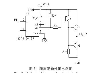
6. Design of optocoupler isolation drive circuitThe regulator has a frequency of up to 100 K and uses a high-speed optocoupler 6N137 and a triode to form an optocoupler-isolated driver circuit that responds quickly to the PWM signal. Isolation drive peripheral circuit shown in Figure 5, 6N137 optocoupler input and output reverse, so the output plus a PNP tube, so that the signal G1/G2 follows the input PWM change, C3 is 0.1UF decoupling capacitor, added to 6N137 light Beside the power supply pins of the coupler. When selecting the type of capacitor, select a capacitor with good high frequency characteristics such as a ceramic capacitor or a tantalum capacitor. The 6th pin VO of the 6N137 optocoupler, the output circuit belongs to the open collector circuit, and must pull up a resistor Rz; between the 2nd pin and the 3rd pin of the 6N137 optocoupler is an LED, which must be connected in series with a current limit. Resistor R34O.
The feedback circuit consists of a magnetic amplifier isolator and a sampling resistor R26.R31. The sampling voltage is isolated and amplified by DCP010505B to obtain a voltage UFB. On the one hand, this voltage is applied as a feedback voltage to pin 1 of SG3525, which is compared with the reference voltage to determine the output. The size of the air ratio, the stable output voltage; another as an aspect of the overvoltage protection circuit is added to the positive input terminal of the error amplifier, the input voltage, the overvoltage protection circuit is composed of a follower and a hysteresis comparator, when the output voltage is greater than the set threshold When the voltage is applied, the protection circuit operates, the LED is illuminated, and SD is high, and the output pulse is turned off. The overcurrent protection circuit consists of a sampling resistor, a magnetic isolation amplifier DCP, and LM324. The sampling resistor uses a precision resistor, and the resistance is relatively small. The magnetic isolation amplifier adopts DCP010512B. After the amplifier amplifies the sampling signal and compares it with the reference voltage, the protection action is the same as the overvoltage protection principle.
8, experimentThe Sepic DC voltage regulator debugging circuit board is divided into an auxiliary power circuit board and a chopper main circuit circuit board. The board components are directly inserted, which is convenient for the experiment to find problems and replace the components in time to correct them. The PWM signal was tested and recorded.
9. ConclusionThe main circuit of Sepic DC voltage regulator is non-isolated design. The driving signal can provide enough driving current to drive the MOSFET quickly, and the driving circuit structure is simple and reliable. The regulator meets the requirements of output voltage reliability, stability, etc. The cost is relatively small.
ZGAR Aurora 3000 Puffs
ZGAR electronic cigarette uses high-tech R&D, food grade disposable pod device and high-quality raw material. All package designs are Original IP. Our designer team is from Hong Kong. We have very high requirements for product quality, flavors taste and packaging design. The E-liquid is imported, materials are food grade, and assembly plant is medical-grade dust-free workshops.
Our products include disposable e-cigarettes, rechargeable e-cigarettes, rechargreable disposable vape pen, and various of flavors of cigarette cartridges. From 600puffs to 5000puffs, ZGAR bar Disposable offer high-tech R&D, E-cigarette improves battery capacity, We offer various of flavors and support customization. And printing designs can be customized. We have our own professional team and competitive quotations for any OEM or ODM works.
We supply OEM rechargeable disposable vape pen,OEM disposable electronic cigarette,ODM disposable vape pen,ODM disposable electronic cigarette,OEM/ODM vape pen e-cigarette,OEM/ODM atomizer device.

Aurora 3000 Puffs,ZGAR Aurora 3000 Puffs Pod System Vape,ZGAR Aurora 3000 Puffs Pos Systems Touch Screen,ZGAR Aurora 3000 Puffs Disposable Vape Pod System,3000Puffs Pod Vape System
ZGAR INTERNATIONAL(HK)CO., LIMITED , https://www.sze-cigarette.com