EMC EMC (ElectromagneTIc compaTIbility)
For the performance index of the equipment or system, literal translation is "electromagnetic compatibility";
However, as a discipline, it should be translated as "electromagnetic compatibility."
The national standard GB/T4365-1995 "Electromagnetic Compatibility Terminology" defines electromagnetic compatibility as "the ability of a device or system to function properly in its electromagnetic environment and does not constitute unacceptable electromagnetic disturbance to anything in the environment."
Simply put, it is the ability to resist interference and the extent of foreign harassment.
Electromagnetic compatibility is a science that studies the effects of coexistence of various electrical equipment (subsystems and systems; broadly including organisms) in a limited space, limited time, and limited spectrum resources without causing degradation.
Second, the basic conceptElectromagneTIc compaTIbility (EMC) Electromagnetic Compatibility - Electronic products can work in an electromagnetic environment without reducing the ability to function or damage;
Electromagnetic interference (EMI) Electromagnetic interference - The process by which electromagnetic energy in electronic products propagates through conduction or radiation; it consists of three elements: interference sources, coupling channels, and interfered receivers.
Radio frequency (RF) Radio frequency, radio frequency - The frequency range used for communications is approximately 10 kHz to 100 GHz. These energies can be intentional, such as an infinite teleporter, or unintentionally produced by an electronic product; RF energy is transmitted via two modes:
Radiated emissions (RE)—The electromagnetic field of such RF energy is transmitted through the medium; RF energy is generally propagated in free space, however, other types may also occur.
Conducted emissions (CE)—Electromagnetic fields of this type of RF energy propagate through the medium of the problem, typically via wires or interconnect cables; Line Conducted Interference (LCI) refers to RF energy on the power line.
Susceptibility, Tolerability—Relatively measures the extent to which a product is exposed to chaos or damage in an EMI environment.
Immunity immunity - a relative measure of product's ability to withstand EMI;
Electrical overstress (EOS) Electronic over-voltage - when it encounters high-voltage surge products suffered damage or just a loss of function; EOS includes lightning and electrostatic discharge events.
Electrostatic discharge (ESD) Electrostatic discharge - a high-voltage pulse wave that may cause damage or loss of function to the affected product. Although lightning strikes are also a high voltage pulse wave, ESD generally refers to a lower amperage and is roughened by the human body. Caused by the trigger; in general, lightning strikes are considered as ESD categories, because the protection is very similar, but the difference in size only.
Radiated susceptibility (RS) Radiation Tolerance - The ability of a product to withstand EMI transmitted through free space.
Conducted susceptibility (CS) Conductive resistance - The ability of a product to withstand electromagnetic energy propagating through external cables, power lines, and other I/O cables;
Containment Closed, encircled—Prevents RF energy from escaping an enclosure, usually in a metal cage or in a plastic enclosure with conductive paint. By mutual principles, we also visually containment to prevent RF energy from entering the enclosure.
Suppression Suppression—Designed to reduce or eliminate RF energy at the source end so that it does not rely on second-order methods such as metal enclosures.
Third, electromagnetic interference source typeThere are many kinds of electromagnetic interference sources and they can be classified according to different methods. The sources of interference that directly affect the measurement and measurement equipment in the measurement environment can be divided into natural and artificial interference sources.
Natural sources of interference include:
(1) Atmospheric noise interference: such as spark discharge generated by lightning, is pulsed broadband interference, which covers from several Hz to 100MHz or more. The spread is quite far.
(2) Solar noise: It refers to the radiation noise of sunspots. During the sunspot activity. The explosion of sunspots. It can generate thousands of times more intense noise than the stationary phase. Causes the communication to be interrupted.
(3) Ning Zhou noise: refers to the noise from the universe.
(4) Electrostatic discharge: Electrostatic voltage accumulated on the human body and equipment can be as high as tens of thousands of volts up to hundreds of thousands. Often discharged by corona or sparks, called electrostatic discharge. Electrostatic discharges generate powerful transient currents and electromagnetic pulses that can damage static-sensitive devices and devices. Electrostatic discharge is a pulse broadband interference, spectrum components from the DC has been continuous sword frequency band.
Sources of human interference refer to electromagnetic interference generated by electrical and electronic equipment and other artificial devices. The man-made interference sources mentioned here refer to unconscious interference. As for the intentional release of interference in order to achieve a certain purpose, such as electronic countermeasures, etc. are beyond the scope of this article.
Any electronic and electrical equipment may cause human interference. Here, only some common interference sources in the interference measurement environment are mentioned.
(1) Radio transmission equipment: including mobile communication systems, radio, television, radar, navigation and radio relay communication systems. Such as microwave relays, satellite communications, etc. Due to the large power emitted, its fundamental signal can produce functional interference; harmonics and spurious emissions constitute non-functional unwanted signal interference.
(2) Industrial, scientific, medical (ISM) equipment: such as induction heating equipment, high-frequency welding machine, X-ray machine, high-frequency physiotherapy equipment, etc. The powerful output power not only interferes with the radiation of space, but also interferes with remote devices through the power frequency network.
(3) Power equipment: Including servo motors, drills, relays, elevators, etc. The sudden change in current generated by the on/off of the equipment and the attendant electric spark becomes a source of disturbance: non-linear loads in electric power systems (eg electric arc furnaces, etc.), intermittent power sources ( UPS) Equivalent power conversion equipment generates a large amount of harmonic influx into the grid and becomes a source of interference: fluorescent devices such as fluorescent lamps also produce glow discharge noise interference.
(4) Ignition systems for automobiles and internal combustion engines: Vehicle ignition systems produce broadband interference, and the interference intensity is almost constant from several hundred kHz to several hundred megahertz.
(5) Grid interference: refers to the interference generated by the powerful electromagnetic field and earth leakage current of the 50Hz AC grid, and the micro arc caused by the poor contact of the high-voltage transmission lines such as corona and insulation fracture, and the spark of the surface of the contaminated conductor.
(6) High-speed digital electronic equipment: Includes computers and related equipment.
The mechanism of the electromagnetic interference source mentioned above is: discharge noise (lightning, electrostatic discharge, glow discharge, etc.). Contact noise, circuit transitions, electromagnetic wave reflections, etc. The reflection of electromagnetic waves in transmission lines is a source of interference that must be taken seriously for high frequency measurements and digital equipment.
Fourth, electromagnetic interference coupling channelThe important factor in electromagnetic interference is the coupling channel. In many cases, it is difficult to find the real interference source, and it is difficult for the interfered receiver to improve. The most feasible solution at this time is to interfere with the interference in the coupling channel. The coupling is fully attenuated.
Fifth, the coupling channel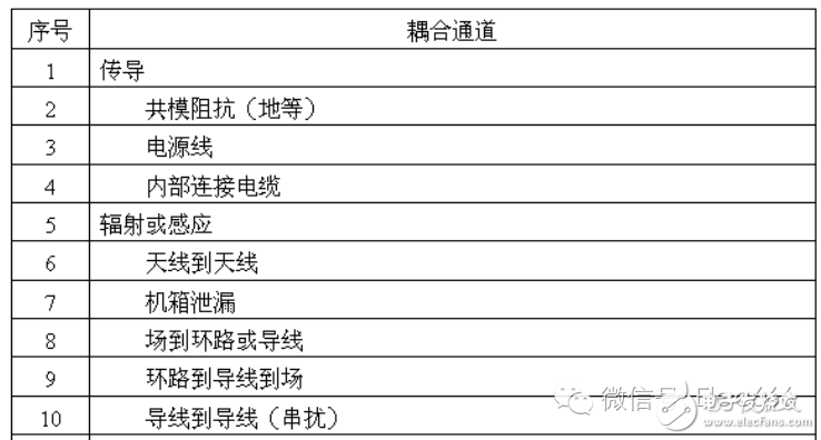
There are two ways of transmission of electromagnetic interference: conduction transmission and radiation transmission. From the perspective of the sensor being disturbed, the coupling of interference can be divided into two types: conductive coupling and radiation coupling.
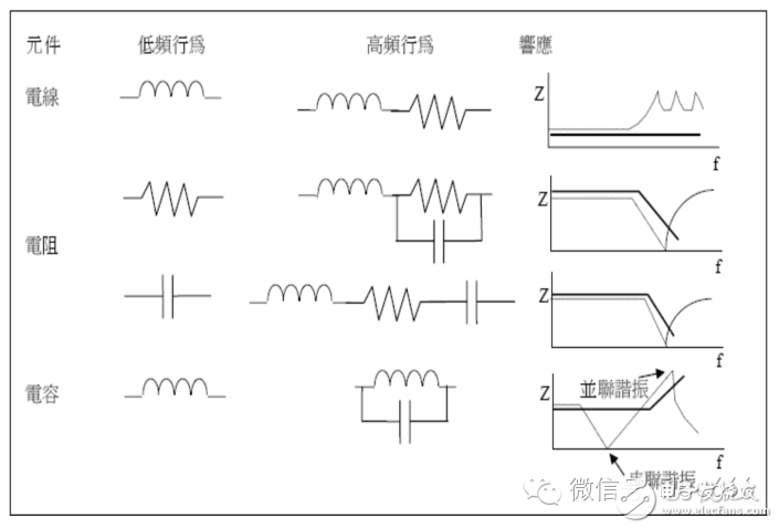 Sixth, the type of conductive coupling
 1. Resistive coupling

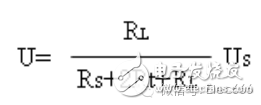
The source of interference is directly coupled to the receiver through the resistance Rt of the wire. Let Us be the interference voltage and Rs the internal resistance of the interference source. The voltage at the receiver is:
2. Capacitive coupling
Circuit A and Circuit B are capacitively coupled through two wires. Also known as electric field coupling.
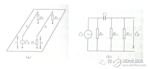
In radio frequency circuits, multi-conductor cables, interference on one conductor can be coupled to all other conductors, so high-frequency signal lines must be shielded. Distributed capacitive coupling is most likely to occur between the pins of the high-frequency amplification transistor, and the lead length of the pins should be minimized.
Inductive coupling
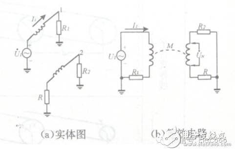
When a variable current flows through a circuit, a variable magnetic field is generated in the space around it. This changed magnetic field generates an induced voltage in an adjacent loop, which couples an interference voltage into the receiving circuit. Inductive coupling is also called magnetic field coupling.
1. Common ground impedance coupling
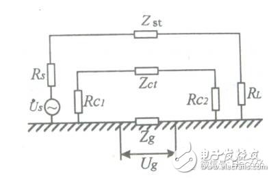
In the figure, Us is the interference source voltage, Rs is the internal resistance of the interference source, RL is the load of the interference source circuit, Zst is the impedance of the connection line of the interference source circuit, Rc1 and Rc2 are the internal resistance and load of the interfered loop, and Zct is the disturbed loop. The connection impedance. Zg is the common ground impedance.
In the interference source loop, there is generally RS+ZST+RL>>Rg, so the loop current I1 can be obtained as:
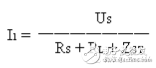
I1 causes interference voltage Ug on the common ground impedance:

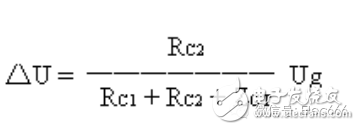
The common ground impedance voltage drop Ug causes an additional disturbance voltage ΔU on the load RC2 in the receiving loop:
2. Total power supply coupling
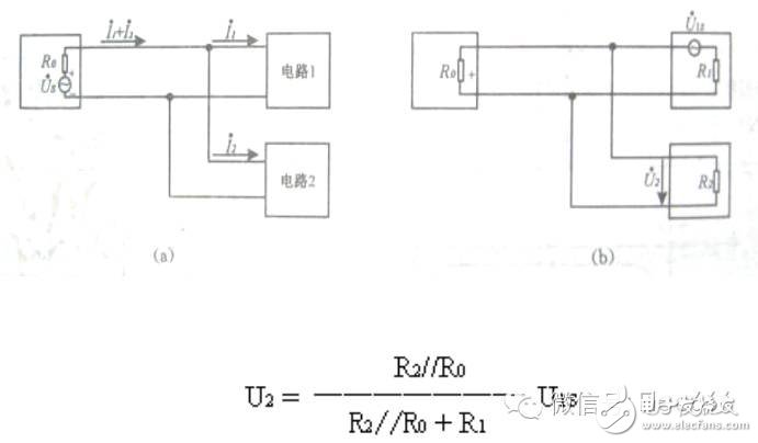
It can be seen that any interference signal generated in the load circuit will be conducted through the internal resistance coupling to other load circuits. As can be seen from the above formula, if R0 = 0, that is, the power supply has no internal resistance, the interference will not be conducted, in fact, the internal resistance of the power supply. It cannot be zero.
VIII. International standards and national standards for electromagnetic compatibilityThere are many international standards relating to electromagnetic compatibility, including the US military standard MIL/ANSIC/AIR, the International Special Committee on Radio Interference (CISPR) standard, the US federal standard FED/FCC, the German standard DIN/VDE, the palce standards C, and the British standard BS. , ISO, CEN, IEC, etc. The current national standards in China are GB/T 17626, GB9254 and GB6833, which correspond to the International Electrotechnical Commission standard IEC 61000.
Nine, EMC test project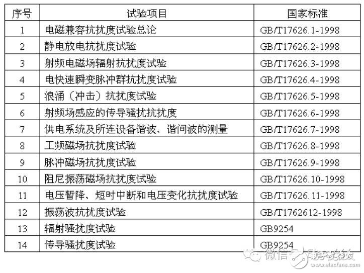
The electrostatic discharge immunity test evaluates the anti-static capability of the equipment and imposes electrostatic interference on the housing of the equipment and the parts of the equipment that can be contacted by the human hand to check whether the equipment can work normally. There are corresponding level requirements and test methods.
The electrical fast transient pulse group immunity test evaluates the anti-pulse interference capability of the equipment, imposes regular pulse interference on the equipment power supply, and checks whether the equipment can work normally. There are corresponding level requirements and test methods.
The surge (impact) immunity test examines the surge immunity of the device, applies high-energy pulse interference to the device power supply, and examines whether the device can function properly. There are corresponding level requirements and test methods. Generally used to assess power.
The radiation disturbance test examines the degree of external radiation interference of the equipment. In the microwave darkroom, a standard antenna is used to receive radiation signals when the equipment is operating. There are corresponding level requirements and test methods.
Conducted harassment test to examine the degree of external conduction interference equipment, in the shielded room inside the standard instrument receiver equipment work from the power line conduction out of the interference signal. There are corresponding level requirements and test methods.
X. Electromagnetic Compatibility MeasuresThe electromagnetic compatibility design of the equipment includes the following steps:
1. Component selection and circuit design
2. Application of filter technology
3. Grounding design
4. Application of shielding technology
5. Circuit layout and equipment layout planning
6. Classification and laying of wires
7. Component Selection and Circuit Design
The source of electromagnetic compatibility is to select the components and circuit design, because the components are both the interference source and the interfered receiver, reduce the electromagnetic interference amplitude of the interference source to the outside, and select the element with strong anti-electromagnetic interference with a suitable cost performance. The device is the most effective way to improve the electromagnetic compatibility performance.
XI. Application of Filtering TechnologyThe interference in the power supply is divided into two kinds: common mode interference and differential mode interference. The interference between the phase line of the power line and the ground line is common mode interference, such as U1 in the figure; the interference between the neutral line and the ground line also has a total Mode interference, such as U2; and the interference between the online phase and the neutral line is called differential mode interference, such as U3. Differential mode interference currents are equal in phase and neutral and are in opposite phase. Common-mode interference exists at the same time in the phase and neutral lines, and they have the same size and phase.
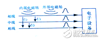
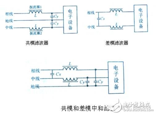
In fact, common mode and differential mode interference are often present in the power line. Therefore, a practical power filter consists of a common mode filter circuit and a differential mode filter circuit, as shown in the figure:
Grounding is intended to mean a connection to the true ground to provide a lightning discharge path. For example, one end of a lightning rod is buried in the ground and later becomes a technical measure for electrical equipment and electrical facilities to provide leakage protection discharge paths.
Now that the meaning of grounding has been extended, it generally refers to a technical activity that is connected to a good conductor as a reference potential point (or surface). The "ground" is not necessarily the actual ground, but refers to a part of the circuit and system. Metal conductive plate line, it can be used as a common potential reference point for any electrical signal in each circuit of the system, the ideal grounding conductor is a zero-resistance entity, any current flowing in the grounding conductor should not produce a voltage drop, the grounding point of each There should be no potential, but electromagnetic interference will be introduced if it is improperly grounded.
Generally, the circuit is divided into four types according to the signal characteristics and grounded separately to form four independent grounding systems. Each "ground" system may adopt different grounding methods.
The first category is sensitive signals and small-signal "ground" systems. Including low-level circuit, weak signal detection circuit, sensor input circuit, pre-amplifier circuit, mixer, etc., due to the low operating level of these circuits, the signal amplitude is weak, especially vulnerable to failure or degradation, so their Lines should not be mixed in other circuits.
The second category is the ground system for insensitive signals and large signal circuits. It includes a high level circuit, a final stage amplifier, a high power circuit, and the like. Because the operating current in these circuits is relatively large, the current in the ground system is also relatively large, so it must be set separately from the ground of the small-signal circuit. Otherwise, the coupling effect of the ground wire will inevitably cause disturbance to the small-signal circuit. Can not work normally.
The third category is the system of interference source equipment, which includes motors, relays, contactors, etc. Since sparks or inrush currents are generated during operation of such components, they often cause serious interference to electronic circuits. In addition to shielding isolation techniques, ground lines must be set separately from electronic circuits.
The fourth category is the metal component ground. It includes chassis, floor, doors, panels, etc. In order to prevent personal electric shock accidents, lightning accidents, external electromagnetic field interference, and static electricity generated by friction, it is necessary to ground the case.
Thirteen, grounding system classification principle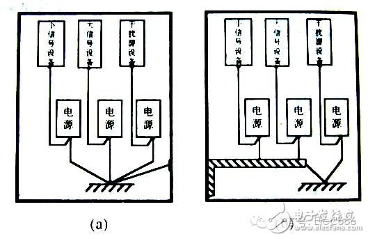
Single point grounding system
In this case, the ground potential of each device (or each branch) is only related to the respective ground current I and ground, and is not affected by other circuits, and is effective in preventing interference between circuits and ground loop interference. . Especially when the circuit frequency is low and the connecting wire is relatively short, this grounding method is often used. Its disadvantage is that it is not suitable for high-frequency circuits.
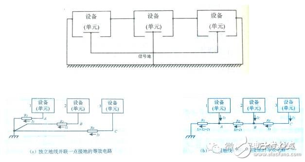
2. Multi-point grounding system
Multi-point grounding refers to the fact that each unit circuit in the device is directly connected to the ground and has multiple grounding points, as shown in the figure. For high-frequency circuits, in order to reduce the ground impedance, a multi-point grounding method is generally adopted. The ground lines used in the figure are respectively connected to the nearest low impedance ground line. The ground wire system is generally a flat metal conductor connected to the casing or the casing itself, and its inductive reactance is very small.
The advantage of a multi-point grounding system is that the circuit configuration is simpler than single point grounding, and because of the short grounding line, the high-frequency standing wave phenomenon that may appear on the grounding line is significantly reduced. However, due to the multi-point grounding, a lot of ground loops will be added inside the device, which will cause interference to lower level circuits and bring about adverse effects.

3. Hybrid grounding system
In some electrical equipment, there are both high frequency and low frequency components. At this point should be treated separately, low-frequency circuit using a single point of grounding, high frequency circuit needs more grounding. This grounding system is called a hybrid grounding system as shown in the figure.
The situation of the actual electrical equipment is more complicated, it is difficult to solve the problem through a simple grounding method, so the hybrid grounding system is more commonly used.

1, electrostatic shielding
Assuming that the conductor A with positive charge is adjacent to the conductor B, the conductor B will be negatively charged due to electrostatic induction as shown in the figure.
If the conductor A is surrounded by a metal shield, an equal amount of negative charge with the conductor A is induced on the inside of the shield and an equal amount of positive charge appears on the outside. The power line will continue to reach B and the induced electric field will be more For complexity. If the metal shield is grounded, the external electric field of the shield disappears and the conductor B will not be subjected to inductive interference. This is the principle of electrostatic shielding.
Electrostatic shielding should have two basic points: perfect shielding and good grounding.

2, magnetic shielding
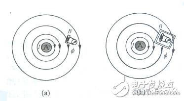
Magnetic shielding is used to isolate the magnetic field. There is a magnetic field around any current-carrying wire or coil. As shown in Figure (a), there is a current I in the wire A. There is a magnetic field around the wire. A series of concentric magnetic lines is used. In order to prevent the magnetic field from interfering with the adjacent element B, B can be surrounded by a material with high magnetic permeability, so that the magnetic lines of force gather in the shield body, so that the sensitive element B is protected, as shown in (b).
Since the magnetic permeability of the magnetic shielding material is several tens of times and several thousand times larger than that of air, most of the magnetic lines of force are concentrated in the shielding layer, so that the element B is free from interference.
The magnetic field shielding is different from the electric field shielding, and the shielding body does not affect the shielding effect because it is not grounded, but since the magnetic shielding material also plays a certain shielding effect on the electric field, it is usually also grounded.
3, electromagnetic shielding
Electromagnetic shielding is an effective method to prevent alternating electromagnetic field induction and radiation interference.
The electromagnetic field is divided into alternating electric field, alternating magnetic field and alternating electromagnetic field. The principle and method of shielding the three fields are different.
1). Alternating electric field shielding
The principle of alternating electric field shielding is to use a well-grounded metal shield to confine the alternating electric field generated by the field source to a certain space, thereby blocking the electric field transmission path between the interference source and the sensitive circuit.
2). Alternating magnetic field shielding
Alternating magnetic field shielding has high frequency magnetic shielding and low frequency magnetic shielding. The principle of low-frequency magnetic shielding is the same as that of static magnetic shielding. The typical application is the encapsulation of the relay, the jacket of the power transformer, and the package of the filter. High-frequency magnetic shielding is the use of the eddy current generated by the shield against the magnetic field, offset interference magnetic field, to achieve the principle of shielding. Therefore, high-frequency magnetic shielding uses highly conductive materials such as copper and aluminum. A typical application is a medium-term transformer in radios.
3). Alternating electromagnetic shielding
Electromagnetic shielding is a technical measure to prevent electromagnetic waves of high-frequency radiation from propagating in space by using a shield, and the shield acts to cut off or impair the transmission of electromagnetic waves.
When the alternating electromagnetic field passes through the metal material shielding body, the metal material generates an induced potential to form a vortex, and the magnetic field generated by the eddy current can cancel out part of the original magnetic field, thereby acting as a shielding effect. The greater the eddy current, the stronger the shielding effect, so the greater the shielding material conductivity, the better the shielding performance. The higher the electromagnetic frequency, the stronger the shielding effect.
15. Electromagnetic Compatibility ImplementationPower supply: Since many electromagnetic interferences are coupled to the electronic equipment through the power supply, special electromagnetic compatibility design is performed on the system power supply. Increase effective transformer, regulator, and filter circuits, use high-efficiency switching power supply chips and low-dropout linear power supply chips with good voltage regulation and filtering to provide a stable and reliable power supply for the system.
2. Use decoupling capacitors: Add a decoupling capacitor between each power supply of the integrated circuit and ground. The decoupling capacitor has two functions: on the one hand, the storage capacitor of the integrated circuit provides and absorbs the charge and discharge energy of the integrated circuit for opening and closing the door; on the other hand, it bypasses the high-frequency noise of the device.
3. Ground separation: The use of 4-layer circuit board design to reduce the parasitic inductance of the power supply and ground effectively enhances the EMC performance of the system. A separate power layer and ground layer can effectively prevent the devices from being coupled to each other through the ground line and the power supply. In addition, the method of splitting and isolating the ground lines with different properties enables the currents of different attributes of the ground lines to go through different paths and prevent Signal crosstalk.
Communication interface: The system's 485, 232, USB and other communication interface external cables, and has direct contact with external devices, so it is also vulnerable to various electromagnetic interference, in order to enhance the anti-interference ability of these communication interfaces, in the communication signal line Magnetic beads and shunt varistors, as well as filter capacitors;
In addition, in order to enhance the noise immunity and reduce the degree of harassment, the following principles should be followed when laying out the PCB board:
1. The quartz crystal oscillator should be as close as possible to the device that uses this clock. The clock line should be as short as possible. The housing should be grounded. Use the ground wire to circle the clock area.
Do not route under quartz crystals and under noise-sensitive devices.
2. The I/O driver circuit should be as close to the printed board as possible, allowing it to leave the printed board as soon as possible. The signal entering the printed circuit board must be filtered, the signal from the high noise area must be filtered, and the signal reflection can be reduced by using the series termination resistor.
3. MCU useless terminal must be connected high, or grounded, or defined as the output terminal, the end of the integrated circuit should be connected to the power supply, do not float. Don't leave unused gates unconnected.
4. The printed board should use 45 fold lines instead of 90 fold lines to reduce the external emission and coupling of high frequency signals.
5. Correctly select single-point grounding and multi-point grounding. In the low-frequency circuit, the operating frequency of the signal is less than 1MHz, and its influence on the inductance between the wiring and the device is small, and the circulation current formed by the grounding circuit has a great influence on the interference, so a point should be grounded. When the operating frequency of the signal is greater than 10 MHz, the impedance of the ground wire becomes very large. At this time, the resistance of the ground wire should be reduced as much as possible, and the multi-point grounding should be used nearby. When the operating frequency is from 1 to 10 MHz, if a point is grounded, the length of the ground wire should not exceed 1/20 of the wavelength. Otherwise, the multi-point grounding method should be adopted.
6. Separate the digital circuit from the analog circuit. There are both high-speed logic circuits and linear circuits on the circuit board. They should be separated as much as possible, and the ground lines of the two should not be mixed. They are connected to the power supply ground. Try to increase the grounding area of ​​the linear circuit.
7. Make the ground wire as thick as possible. If the grounding wire is very fine, the grounding potential changes with the change of the current, causing the timing signal level of the electronic equipment to be unstable and the anti-noise performance to deteriorate. Therefore, the ground wire should be as thick as possible so that it can pass three times the allowable current of the printed circuit board. If possible, the width of the ground wire should be greater than 3mm.
8. Make the ground wire a closed loop. When designing a printed circuit board ground system consisting of only digital circuits, making the ground wire a closed loop can significantly improve the noise immunity. The reason lies in the fact that there are many integrated circuit components on the printed circuit board, especially when there are many components that consume more power, due to the limitation of the thickness of the grounding wire, a large potential difference will be generated in the ground junction, resulting in a decrease in the anti-noise ability. If the grounding structure is looped, the potential difference will be reduced and the anti-noise capability of the electronic equipment will be improved.
9. Choose a reasonable wire width. Because the impact interference produced by the transient current on the printed lines is mainly caused by the inductance components of the printed conductors, the inductance of the printed conductors should be minimized. The inductance of a printed conductor is proportional to its length and inversely proportional to its width, so a short, fine conductor is good for suppressing interference. Clock lines, row drivers, or bus driver signal lines often carry large transient currents. Printed conductors must be as short as possible. For discrete component circuits, when the width of the printed conductor is about 1.5mm, it can fully meet the requirements; for integrated circuits, the width of the printed conductor can be chosen between 0.2~1.0mm.
10. Use the correct cabling strategy. Equivalent traces can reduce the inductance of the wire, but the mutual inductance and distributed capacitance between the wires increase. If the layout allows, it is better to adopt the grid structure of the grid structure. The specific approach is to laterally route one side of the printed circuit board, and the other is to make vertical wiring. Then connect them with metallized holes at the cross holes. In order to suppress the crosstalk between printed circuit board conductors, it is necessary to avoid long-distance equal alignment when designing the wiring.
1.ANTENK Flexible Printed Circuit (FPC) and Flexible Flat Cable (FFC) connectors are ZIF (zero insertion force) and LIF (low insertion force) connectors designed to provide a fast, easy, reliable method to make a connection of flexible printed circuits to a PCB. Adam Tech`s special contact design completely preserves conductor integrity by eliminating all wiping action while making connection. Flex circuitry enters the connector and the connector cap is pressed down to capture the flex circuit producing a stable, high pressure connection. Raising the cap releases the pressure for exchange or replacement of circuitry. This series includes single and dual row versions in thru-hole or SMT mounting in vertical or horizontal orientations.
2.Our products are widely used in electronic equipments,such as monitors ,electronic instruments,computer motherboards,program-controlled switchboards,LED,digital cameras,MP4 players,a variety of removable storage disks,cordless telephones,walkie-talkies,mobile phones,digital home appliances and electronic toys,high-speed train,aviation,communication station,Military and so on
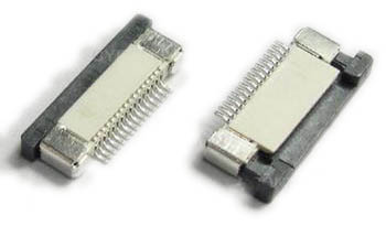
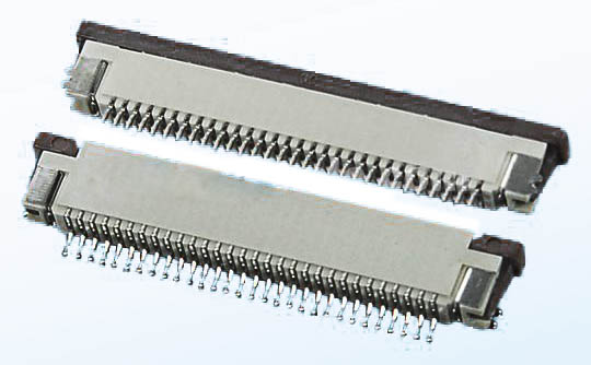
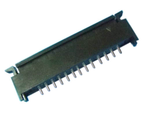
FFC Connector Range Available as:
0.3,0.5, 0.8, 1.0,1.25, 2.54mm connector pitch
Surface mount
Side and Top entry
Side entry parts - Top and bottom contact options
ZIF (Zero Insertion Force)
Slide and flip lock actuator styles
Specifications:
Material And Finish:
Insulator: LCP
Lock: PPS
Insert Spring:Phosphor Bronze,
Matte Tin Plated
Solder Platten Area:Phosphor
Bronze,Matte Tin Plated
Voltage:500 V AC(rms)/DC
Current:0.5 A AC(rms)/DC
Contact Resistance:20 mΩ max(initial)
Insulation Resistance:800 MΩ min
Operating Temp:-20°-85°
Fpc Connector,Fpc Cable Connectors,Ffc Cable Connectors,Pitch Fpc Connector,Surface mount FPC/FFC Connectors,Top entry FFC Connectors, Side entry FFC Connectors
ShenZhen Antenk Electronics Co,Ltd , https://www.antenkwire.com