The internal architecture of the ASIC chip is relatively simple. It cannot be programmed with hardware. It can only be used to specifically deal with certain functions, but it has the lowest flexibility, but it is most efficient in performing certain tasks. ASICs are also known as application specific integrated circuits.
You can think of fpga as putting a bunch of logic devices such as an AND gate, an OR gate, a selector, etc. in a box. The box is surrounded by the pins of the film. Through logic programming, many gates and many selectors and other devices are connected in series or in parallel. It's equal to doing electrical experiments in fpga.
FPGA features are as follows:
(1) Using FPGA to design ASIC circuits (application-specific integrated circuits), users do not need to shoot to produce chips that can be used together.
(2) FPGAs can be used as mid-samples for other full-custom or semi-custom ASIC circuits.
(3) The FPGA has a rich set of flip-flops and I/O pins.
(4) FPGA is one of the devices with the shortest design cycle, lowest development cost, and lowest risk in ASIC circuits.
(5) FPGA adopts high-speed CMOS technology, low power consumption, and can be compatible with CMOS and TTL levels.
The internal structure of the CPU chip is the most complex and cannot be programmed by hardware. However, software that implements various functions can be written by an external programming software, which has the highest flexibility and the lowest processing efficiency. The CPU is also called a universal integrated circuit.
PLDPLD is short for Programable Logic Device. FPGA is short for Field Programable Gate Array. The functions of the two are basically the same, but the implementation principle is slightly different, so we can sometimes ignore this. The difference between the two is collectively referred to as a programmable logic device or a PLD/FPGA. PLD is the most dynamic and promising technology in the field of electronic design. Its influence is no less than the invention and use of the single chip microcomputer in the 1970s.
What can PLD do? It is no exaggeration to say that PLDs can perform the functions of any digital device, from high performance CPUs down to simple 74 circuits, and can be implemented using PLDs. PLD is like a piece of white paper or a stack of wood. Engineers can design a digital system freely through the traditional schematic input method or hardware description language. Through software simulation, we can verify the correctness of the design in advance. After the PCB is completed, the online modification capability of the PLD can also be used to modify the design at any time without changing the hardware circuit. Using PLDs to develop digital circuits can greatly reduce design time, reduce PCB area, and increase system reliability. These advantages of PLD make PLD technology develop rapidly after 1990s, and also greatly promote the progress of EDA software and Hardware Description Language (HDL).
How to use PLD? In fact, the use of PLD is very simple. Learning PLD is much simpler than learning a single-chip microcomputer. Based on digital circuits, computers can be used to develop PLDs. Friends who are not familiar with PLD can take a look at the development of programmable logic devices. Today's society is a digital society. It is a society where digital integrated circuits are widely used. The digital integrated circuit itself is constantly being updated. It has evolved from early electron tubes, transistors, small and medium scale integrated circuits, to very large scale integrated circuits (VLSIC, tens of thousands of gates), and many specialized integrated circuits with specific functions.
However, with the development of microelectronics technology, the task of designing and manufacturing integrated circuits has not been fully borne by semiconductor manufacturers. System designers are more willing to design their own application specific integrated circuit (ASIC) chip, and hope that the ASIC design cycle is as short as possible. It is best to design the appropriate ASIC chip in the laboratory and immediately put it into practical use. As a result, Field Programmable Logic Devices (FPLDs) have emerged, of which the most widely used are Field Programmable Gate Arrays (FPGAs) and Complex Programmable Logic Devices (CPLDs). Early programmable logic devices were only programmable read-only memory (PROM), ultraviolet (UV) erasable EPROM, and EEPROM (Electronically Erasable Read Only Memory).
Due to structural constraints, they can only perform simple digital logic functions. Since then, there has been a class of slightly more complex programmable chips, programmable logic devices (PLDs), that can perform a variety of digital logic functions. A typical PLD consists of an AND gate and an OR gate array, and any combinatorial logic can be described by a AND and OR expression. Therefore, the PLD can perform a large amount of combinatorial logic in the form of a product sum. Features. The products of this stage mainly include PAL (Programmable Array Logic) and GAL (Universal Array Logic).
The PAL consists of a programmable AND plane and a fixed OR plane, or gates. The output can be selectively placed in the registered state by the trigger. The PAL device is field-programmable and its implementation process includes anti-fuse technology, EPROM technology, and EEPROM technology. Another class of more flexible logic devices is the programmable logic array (PLA). It also consists of an AND plane and an OR plane, but the connection relationship between these two planes is programmable. PLA devices are both field-programmable and mask-programmable. On the basis of PAL, we have also developed a generic array logic (GAL) such as GAL16V8, GAL22V10 and so on. It adopts EEPROM technology, and realizes electric depressing and electric rewriting. Its output structure is a programmable logic macro unit. Therefore, its design has a great flexibility and is still used by many people. A common feature of these early PLD devices was the ability to implement logic functions with better speed characteristics, but their overly simple structure also allowed them to implement smaller circuits.
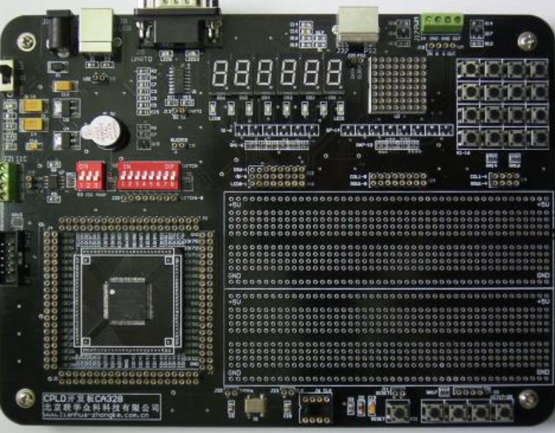
CPLDCPLD is the abbreviation of Complex Programmable Logic Device. Chinese is a complex programmable logic device. It is a device developed from PAL and GAL devices. It has a large scale and a complicated structure and belongs to the scope of large-scale integrated circuits. CPLD is a digital integrated circuit that users construct their own logic functions according to their own needs. The basic design method is to use the integrated development software platform, using the schematic, hardware description language and other methods to generate the corresponding target file, the code is transmitted to the target chip through the download cable to achieve the design of the digital system.
In the 1970s, the earliest programmable logic device PLD was born. Its output structure is a programmable logic macro unit, because its hardware structure design can be completed by software (equivalent to artificially designing the partial indoor structure after the house is covered), so its design is more flexible than the pure hardware digital circuit. , but its overly simple structure also allows them to implement smaller circuits. In order to make up for the defect that PLDs can only design small-scale circuits, CPLDs, a complex programmable logic device, were introduced in the mid-1980s. This application has in-depth network, instrumentation, automotive electronics, CNC machine tools, aerospace measurement and control equipment.
CPLD is a digital integrated circuit that users construct their own logic functions according to their own needs. The basic design method is to use the integrated development software platform to generate the corresponding target file by means of schematics, hardware description languages, etc. The code is transmitted to the target chip through the download cable (programmed in the system) to realize the designed digital system. .
CPLD is small and fast, but it has few resources. CPLD is an abbreviation of Complex Programmable Logic Device. It represents a kind of programmable logic device. It can be defined by the user according to their own needs after the manufacturing is completed. No external RAM is required.
Let's talk about FPGAs and CPLDs. First understand the name. FPGA: Field Programmable Gate Arrays, CPLDs: Complex Programmable Logic Devices. They are all programmable devices, but the CPLD program is solidified in the internal flash. The power-up procedure is still there. There is no internal flash in the FPGA. After the power is turned off, the program will disappear. Of course, an external flash memory program can be attached to the FPGA. Each time the power is turned off and restarted, the flash is loaded. From the scale, the FPGA's capacity (logical unit) is generally much larger than the CPLD, more powerful, higher cost, greater power consumption, programmability is also more flexible, so the two have different market positioning FPGAs are mainly used in chip functional verification (highly complex), image processing (big data), and communications (high-rate) fields. CPLDs can be used in small-scale industrial control markets such as signal generation.
PLD is a broad concept, FPGA and CPLD belong to PLD, programming is hardware programmable, logic design! PLC is a programmable controller, the common 51 single-chip microcomputer belongs to PLC, is ASIC! That is, the hardware is dead, the internal circuit is solidified and can be seen as a custom chip, and programming is software programming!
DSP has a strong computing power, there are more multiplier adder, etc. Strictly speaking, DSP is a kind of soft core, and then increase the external storage, clock, etc. before packaging into a chip, in the image processing, mathematical operations have a comparison Great advantage.
From the earliest PAL, GAL development to later CPLD, FPGA, belong to the programmable logic device.
The internal construction of these devices varies, but overall, they are similar to the type of breadboard used for experiments.
On the breadboard, we can insert various devices and use flying wires to connect them into various circuits.
The same is true for programmable devices. There are two major parts: a large number of pre-made logic gates, flip-flops, memories, etc., as well as the wiring connected to them. The connection point between the wiring and the wiring is empty, and the connection point between certain wirings may be connected or disconnected by some means, so that a circuit connection is established between various pre-made devices to complete a certain function. The process is called "programming."
Some devices are disposable and short-circuit or open circuit between circuits at one time. Some use a transmission gate to connect two lines. The control end of the transmission gate corresponds to one bit in the SRAM or Flash memory, and 1 turns on and the like is disconnected. This memory constitutes the configuration area of ​​the device. Writing specific data into this configuration area can form the required circuit.
As for how to get this configuration data, a simple PAL or GAL can be written by oneself. Large-scale devices can be described by circuit diagrams, logic expressions, hardware description languages, etc., and then synthesized and wired by EDA software to generate the final result. Configuration information, also known as netlist files.
The internal structure of the FPGA chip is slightly more complicated and can be programmed with hardware. Therefore, the logic structure of the internal chip can be changed through a hardware programming language, so that while providing a certain degree of flexibility, it can also ensure a high processing efficiency, which is inflexible and Performance has taken a compromise. FPGAs are also known as programmable integrated circuits.
4G Cat4 Cpe,Mini Soho Portable 4G Cpe,4G Lte Router,4G Volte Router
Shenzhen MovingComm Technology Co., Ltd. , https://www.movingcommiot.com