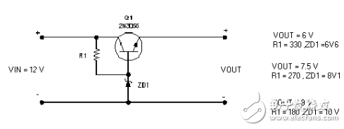
The following figure shows a simple DCDC step-down circuit using the power transistor 2N3055. Different resistors R1 and Zener diodes can be used to adjust the output voltage. The output current may be about 1-2A.
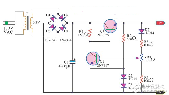
The following figure is a circuit diagram of a linear regulator power supply using a power transistor. The 2N3055 can be replaced by other transistors of the same specification. The 2N3417 can be used with BD139 or other transistors. The diode 1N914 can also be used with a common diode 1N4148. T1 uses 220V (or 110V) 6V to 7V transformer. If the transformer uses 1-2A output current, the output current of the circuit is about 1A.
Inductor buck DC/DC converter: circuit block diagram as shown.
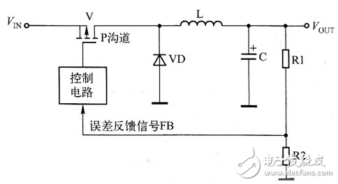
Figure inductive step-down DC/DC converter functional block diagram
In the figure, VIN is the input voltage, VOUT is the output voltage, L is the energy storage inductance, VD is the freewheeling diode, C is the filter capacitor, R1, R2 are the voltage divider resistors, and the error feedback signal FB is generated after the voltage division. Stable output voltage and adjusted output voltage level. The power switch tube V can be either an N-channel insulated gate field effect transistor (MOSFET) or a P-channel FET. Of course, an NPN transistor or a PNP transistor can also be used. In practical applications, a P-channel FET is generally used. Mostly.
The basic operating principle of the buck DC/DC converter is that the V switch operates in the switch state under the control of the control circuit. When the switch is turned on, the FIN voltage forms a loop through the switch S, D poles, energy storage inductance L and capacitor C. The charging current not only establishes a DC voltage across C, but also produces left and right negative inductances on the energy storage inductor L. The electromotive force; During the cut-off period of the switch, since the current in the energy storage inductance L cannot mutate, L generates a right-positive and left-negative pulse voltage through the self-inductance. Then, the positive voltage of right L→filter capacitor C constitutes a discharge loop at the left end of freewheeling diode VD→L, and the discharge current continues to establish a DC voltage at both ends of C. The DC voltage obtained at both ends of C provides power for the load. Therefore, the output voltage generated by the step-down DC/DC converter is not only small in ripple but also in rain and low in the peak voltage of the switching transistor.
Transistor 2N3055 simple DCDC step-down circuit diagram (4) 2n3055 audio power amplifier circuit diagramThe audio power amplifier circuit is simple and low cost. The best power supply voltage is about 50V, but this circuit can work from 30 to 60V. The maximum audio input voltage is about 0.8 - 1V, and the output power is about 60W. The last stage transistor 2N3055 can be any NPN type power transistor, but do not use the Darlington type.
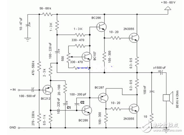
Capacitor C1 adjusts the low frequency (bass), and as the capacitance increases, the low frequencies get louder and louder.
Capacitor C2 regulates a higher frequency (high tone) and becomes louder and louder at higher frequencies as the capacitance increases.
This is a class B amplifier, which means that the push-pull output transistor must apply a quiescent current, even if there is no input signal. This current can adjust the 500Ω trim resistor setting.
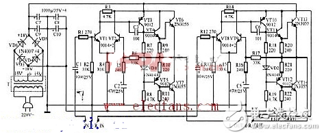
Transistor 2N3055 simple DCDC step-down circuit diagram (5)OCL stereo amplifier circuit
As can be seen from Figure 1, the speaker and amplifier output is directly coupled, in the middle to save the DC output capacitor, in order to make the circuit output terminal voltage zero volts, to take a positive and negative symmetrical power supply, differential amplifier input And other measures. In Figure 1, vTI and vt2 are differential amplification input stages, vt3 is the excitation stage, and vt4~vt7 are the complementary complementary output stages. The audio signal is sent to the base of vTI via the coupling capacitors c1 and ri. After amplification, it is output by the collector of vTI and sent to vt3 to be further larger. The excitation signal output by the vt3 collector drives the power output stage vt4 to vt7. This power-amplified audio signal can drive speaker operation.
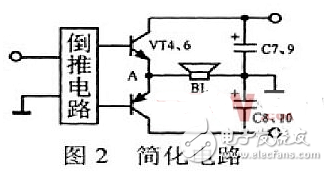
To facilitate further analysis, Figure 1 can be simplified to the form of Figure 2. The combination of vt4 and vt6 is equivalent to an npn transistor, and vt5 and vt7 are compound equivalents of a pnp transistor. From the circuit of Figure 3, vt4, 6 and vt5, 7 and the power supply filter capacitors c9, c10, they are equivalent to one bridge. When vt4, 6, vt5, 7 are all the same, c9, c10 are also identical, the arm balances, the loudspeaker does not have direct current through. If the two positive and negative power supplies are completely symmetrical, then the potential at the output terminal can be guaranteed to be zero volts.
Since the circuits are all directly coupled, any change in ambient temperature and component parameters will affect the potential at the output (point a, Figure 2). To this end, vt1 and vt2 constitute a differential amplifier to overcome zero drift. The circuit also applies DC negative feedback, ie, the output is added to the base of vt2 via r6, which ensures that the potential at the output (point a) is zero volts. . The feedback process is: a point potential ↑ ube ube2 ↑ ie ie2 ↑ ur ur4 ↑ u ubel ↓ icl ↓ uc1 ↑ ube3 ↓ IE2 ↓ ur7 ↓ ube4, 6 ↓ (ube5, 7 ↑) 一 vt4, 6 internal resistance (vt5, 7 internal resistance) a point potential ↓. On the other hand, if point a has a potential of ↓, the potential at point a will be changed by the opposite process.
The choice of components
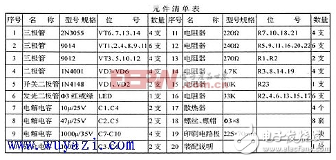
The output stage selects imported high-quality high-power transistor; 2n3055, β value is as high as possible, the rest of the transistors use South Korea imported transistors 9014 and 9012, vd3 ~ vd6 use bridge 1N4001, vd1, vd2 use 1N4148. Power filter capacitors c7 ~ c10 use the electrolytic capacitor 1000μ/35v, the rest of the components see the list of components.
debugging
The power transformer used in this circuit must be prepared by itself, using a center-tapped double output transformer (AC:15V & TImes; 2), with a power of at least 40 watts, connected to the AC- and upper part of the printed circuit board, and then connected to both C9 and C10 after power-on. The end produces a ±18v DC voltage and the voltage across the speaker is zero volts. First, the currents of the differential amplifiers vtl and vt2 are adjusted. In order to avoid a large current flowing through the power tube, the bases of the vt4 and the vt5 are first short-circuited by the wires, and the vt4 to the vt7 are turned off. Then connect the end of resistor r6 to the output and ground it. The total emitter current of the differential amplifier stage is determined by r4. Adjust R4 so that the total emitter current of vt1 and vt2 is 1 mA. After the resistor r6 is restored, the voltage across the speaker should be o. If there is an offset, adjust r3.
Ningbo Autrends International Trade Co.,Ltd. , https://www.vapee-cigarettes.com