Solar energy is an inexhaustible renewable energy source for mankind. It is also clean energy and does not cause any environmental pollution. Among the effective utilization of solar energy, the utilization of solar energy is the fastest growing and most dynamic research field in recent years, and it is one of the most eye-catching projects.
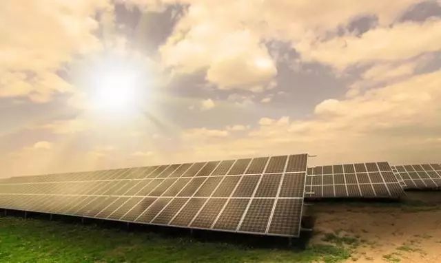
Solar energy is a kind of radiant energy, which must be converted into electrical energy with the help of a pre-energy converter. This energy converter that converts solar energy (or other light energy) into electrical energy is called a solar cell.
The basic working principle of solar cells
The working principle of solar cells is based on the "photovoltaic" effect of semiconductor pn junctions. The so-called photovoltaic effect, to put it simply, is an effect in which the charge distribution state in the body changes when an object is exposed to light to produce electromotive force and current.
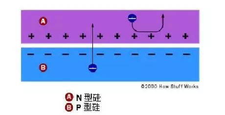
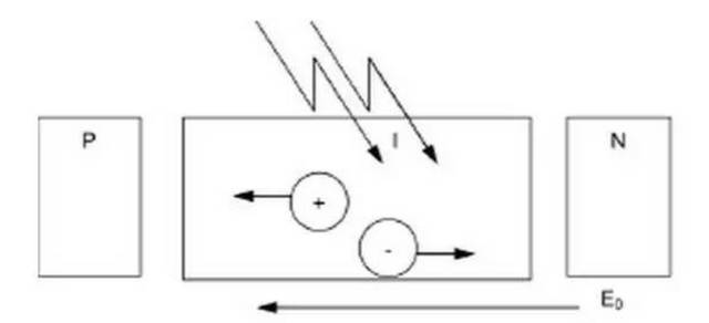
When sunlight or other light irradiates the PN junction of the semiconductor, electron-hole pairs are generated. The carriers generated near the PN junction inside the semiconductor are not recombined but reach the space charge region. Attracted by the internal electric field, electrons flow into n In the region, holes flow into the p region, resulting in excess electrons in the n region and excess holes in the p region. They form a photogenerated electric field that is opposite to the direction of the barrier near the pn junction.
In addition to partially offsetting the effect of the barrier electric field, the photogenerated electric field also makes the p-zone positively charged and the n-zone negatively charged, and an electromotive force is generated in the thin layer between the n-zone and the p-zone, which is the photovoltaic effect. When energy is added to pure silicon (for example in the form of heat), it causes several electrons to break away from their covalent bonds and leave the atom.
Every time an electron leaves, a hole is left. Then, these electrons will wander around the lattice, looking for another hole to settle down. These electrons are called free carriers, and they can carry current.
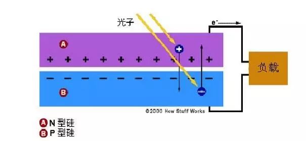
This electric field is equivalent to a diode, allowing (or even pushing) electrons to flow from the p-side to the n-side, not the other way around. When light strikes a solar cell in the form of photons, its energy causes electron-hole pairs to be released. Each photon that carries enough energy usually releases exactly one electron, creating a free hole.
If this happens close enough to the electric field, or free electrons and free holes are just within its influence, the electric field will send electrons to the N side and holes to the P side. This will lead to further destruction of electrical neutrality. If we provide an external current path, electrons will pass through the path and flow to their original side (P side), where they merge with the holes sent by the electric field, and are in the process of flowing. In doing work. Thus, a current flows from the N-type region to the P-type region. Then a potential difference is formed in the PN junction, which forms a power source.
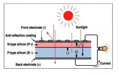
Since semiconductors are not good conductors of electricity, if electrons flow in the semiconductor after passing through the p-n junction, the resistance is very large and the loss is very large. However, if the upper layer is completely coated with metal, sunlight cannot pass through and current cannot be generated. Therefore, metal grids are generally used to cover the p-n junction (such as comb-shaped electrodes) to increase the area of ​​incident light.
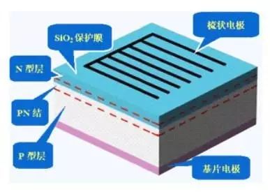
In addition, the surface of silicon is very bright and will reflect a lot of sunlight, which cannot be used by the battery. To this end, scientists coated it with a protective film with a very small reflection coefficient, reducing the reflection loss to 5% or less. After all, the current and voltage that a battery can provide is limited, so people use many batteries in parallel or in series to form solar photovoltaic panels.
Solar cells generate electricity based on the photoelectric properties of specific materials. Black bodies (such as the sun) radiate electromagnetic waves of different wavelengths (corresponding to different frequencies), such as infrared, ultraviolet, visible light, and so on. When these rays are irradiated on different conductors or semiconductors, photons interact with free electrons in the conductors or semiconductors to generate electric current.
The shorter the wavelength and the higher the frequency of the rays, the higher the energy they have. For example, the energy of ultraviolet rays is much higher than that of infrared rays. However, not all wavelengths of radiation energy can be converted into electrical energy. It is worth noting that the photoelectric effect has nothing to do with the intensity of the radiation. Only when the frequency reaches or exceeds the threshold that can produce the photoelectric effect, the current can be generated.
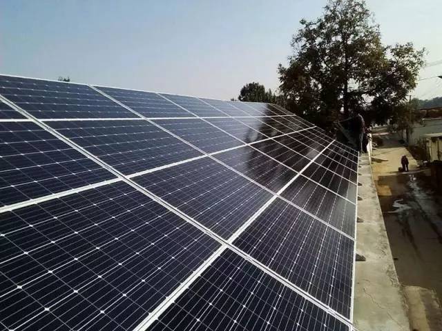
Solar cell power generation is a renewable and environmentally-friendly power generation method. During the power generation process, carbon dioxide and other greenhouse gases will not be generated, and will not cause pollution to the environment.
Types of solar cells
Solar cells can be divided into rigid solar cells and flexible solar cells according to their morphology; according to their crystalline state, they can be divided into two categories: crystalline thin-film and amorphous thin-film, and the former is divided into single crystalline and polycrystalline; according to material It can be divided into silicon film type, compound semiconductor film type and organic film type; according to the different materials used, it can also be divided into: silicon solar cells, multi-compound thin film solar cells, polymer multilayer modified electrode solar cells, nanocrystalline solar cells Batteries, organic solar cells. Among them, silicon solar cells are currently the most mature and occupy a dominant position in applications.
Silicon solar cell
Silicon solar cells are divided into monocrystalline silicon solar cells, polycrystalline silicon thin film solar cells and amorphous silicon thin film solar cells.
Monocrystalline silicon solar cell
The structure of a monocrystalline silicon solar cell mainly includes a front comb-shaped electrode, an anti-reflection film, an N-type layer, a PN junction, a P-type layer, and a back electrode. Monocrystalline silicon solar cells are widely used in space and on the ground. This type of solar cell uses high-purity monocrystalline silicon rods as raw materials. The monocrystalline silicon rod is cut into pieces, and a PN junction is formed through a series of semiconductor processes.
Then the grid lines are made by screen printing method, and the back electrode is made by the sintering process, and the single crystal silicon solar cell is made. The single chips can be assembled into solar cell modules (solar panels) in series and in parallel according to the required specifications to form a certain output voltage and current. Finally, the frame is used for packaging, and the solar cell modules are formed into various solar cell arrays of different sizes.
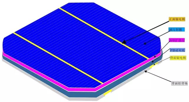
Among the silicon solar cells, monocrystalline silicon solar cells have the highest conversion efficiency and the most mature technology. High-performance monocrystalline silicon cells are based on high-quality monocrystalline silicon materials and related thermal processing techniques.
At present, the electrical technology of monocrystalline silicon is almost mature. In the production of batteries, surface texturing, emitter passivation, zone doping and other technologies are generally used. The developed batteries mainly include planar monocrystalline silicon cells and groove-buried cells. Gate electrode single crystal silicon cell.
The improvement of conversion efficiency mainly depends on the surface microstructure treatment of single crystal silicon and the zone doping process. At present, the photoelectric conversion efficiency of monocrystalline silicon solar cells is about 15%, and the laboratory results are more than 20%.
Features of monocrystalline silicon solar cells
The conversion efficiency of monocrystalline silicon solar cells is undoubtedly the highest, and it still occupies a dominant position in large-scale applications and industrial production. Although its conversion efficiency is high, the production of monocrystalline silicon solar cells requires a large amount of high-purity silicon materials and the process is complicated. The power consumption is very large, and the solar cell module plane utilization rate is low, resulting in the high cost of monocrystalline silicon. It is very difficult to drastically reduce its cost.
In order to save high-quality materials and look for alternatives to monocrystalline silicon cells, thin-film solar cells are now being developed. Among them, polycrystalline silicon thin-film solar cells and amorphous silicon thin-film solar cells are typical representatives.
Polycrystalline silicon solar cell
Polycrystalline silicon thin-film solar cells grow polycrystalline silicon thin films on low-cost substrate materials, using a relatively thin crystalline silicon layer as the active layer of the solar cell, which not only maintains the high performance and stability of the crystalline silicon solar cell, but also the amount of material used Significantly reduced, significantly reducing the cost of the battery. The working principle of polycrystalline silicon thin-film solar cells is the same as other solar cells. The photovoltaic effect is formed based on the action of sunlight and semiconductor materials.
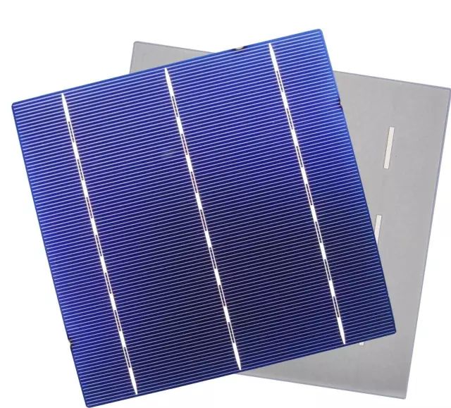
Polycrystalline silicon solar cell chips are semiconductor devices with a photoelectric effect. The PN junction of the semiconductor generates current after being irradiated with light. When the light shines directly on the solar cell chip, part of it is reflected and part of it is absorbed. A part of the electrons in the high-energy state that are bound through the battery chip and absorbed light excites them to become free electrons. These free electrons move in all directions within the crystal, leaving holes (the previous position of the electron). Holes also drift around the crystal. Free electrons (-) accumulate in the N junction, and holes (+) accumulate in the P junction. When the outer loop is closed, current is generated.
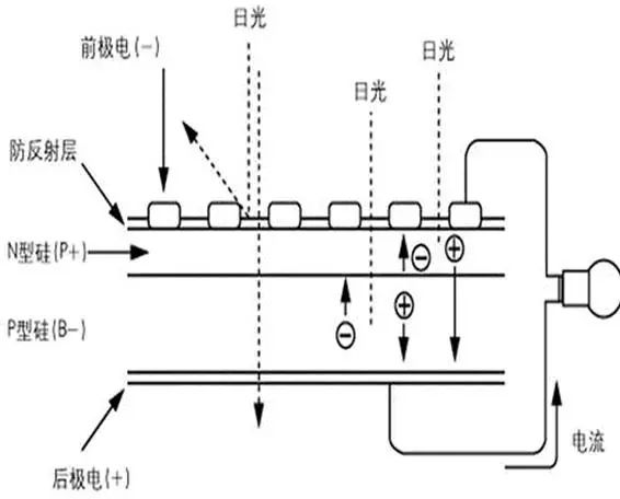
Most of the polycrystalline silicon materials used in solar cells are aggregates containing a large number of single crystal particles, or are melted with waste single crystal silicon materials and metallurgical grade silicon materials, and then injected into graphite molds, that is, polycrystalline silicon ingots. This silicon ingot is cast into cubes for slicing and processing into square cells.
The production process of polycrystalline silicon solar panels is similar to that of monocrystalline silicon solar panels. Its photoelectric conversion efficiency is about 12%, which is slightly lower than that of monocrystalline silicon solar cells. However, the material is easy to manufacture, saves power consumption, and has a lower total production cost. So it has been developed a lot.
Characteristics of polycrystalline silicon solar cells
1. It has stable and efficient photoelectric conversion efficiency.
2. The surface is covered with dark blue silicon nitride anti-reflection film, the color is uniform and beautiful.
3. High-quality silver and silver-aluminum pastes ensure good conductivity, reliable adhesion and good electrode solderability.
4. High-precision screen printing graphics and high flatness make the battery easy for automatic welding and laser cutting.
Amorphous silicon solar cell
Amorphous silicon solar cells are composed of a transparent oxide film (TCO) layer, an amorphous silicon film PIN layer (I layer is intrinsic absorption layer), and a back electrode metal film layer. The substrate can be aluminum alloy, stainless steel, special plastics, etc. It is completely different from the manufacturing method of monocrystalline silicon and polycrystalline silicon solar cells, and consumes less silicon material and lower power consumption.
There are many manufacturing methods, and the most common is to obtain an N-type or P-type amorphous silicon film by the glow discharge method. The substrate material is generally glass or stainless steel plate. Amorphous silicon solar cells are very thin and can be made into a laminated type, or can be manufactured by an integrated circuit method, and multiple cells in series can be fabricated at a time to obtain a higher voltage.
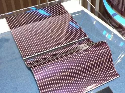
Amorphous silicon, its atomic structure is not arranged regularly like crystalline silicon, but a semiconductor with an amorphous crystal structure. Amorphous silicon is a direct-banding material and has a high solar absorption coefficient. It only needs a 1 um thick film to absorb 80% of the sunlight.
The low cost of amorphous silicon thin film solar cells is convenient for mass production. Insufficient silicon raw materials and rising prices have promoted the efficient use of silicon technology and the development of amorphous silicon thin-film solar cells. The low cost of amorphous silicon thin-film batteries makes up for their shortcomings in photoelectric conversion efficiency, and will occupy an increasingly important position in photovoltaic power generation in the future.
However, due to the many defects of amorphous silicon, the efficiency of the prepared solar cell is low, and the efficiency of the solar cell will decrease with the light, which limits the application of the amorphous silicon thin film solar cell.
At present, the main research direction of amorphous silicon thin film batteries is to combine with microcrystalline silicon to generate amorphous silicon/crystalline silicon heterojunction solar cells. This kind of battery not only inherits the advantages of amorphous silicon batteries, but also can delay amorphous silicon batteries. The efficiency varies with the rate of light attenuation, and the current highest conversion efficiency of pure amorphous silicon thin-film batteries is 17.4%.
Characteristics of amorphous silicon thin film solar cells
Compared with crystalline silicon solar cells, amorphous silicon thin-film solar cells have the advantages of light weight, simple process, low cost, low energy consumption, and convenient mass production. Therefore, they have attracted people's attention and have been rapidly developed. Amorphous silicon thin-film solar cells are the first to be commercialized, and they are currently the largest thin-film cells in the industry.
Although amorphous silicon thin-film solar cells have been extensively researched and applied. However, there are still many problems that need to be solved:
1. The optical forbidden band width of y is 1.7 eV, which makes the material itself insensitive to the absorption of the long wave region of the solar radiation spectrum, which limits its photoelectric conversion efficiency;
2. The photoelectric conversion efficiency weakens with the increase of the light time, the so-called light-induced degradation (SW) effect, which makes the battery performance unstable;
3. During the preparation process, the deposition rate of amorphous silicon is low, which affects the commercial production of amorphous silicon thin-film solar cells;
4. Difficulties in subsequent processing of battery components, such as the handling of Ag electrodes;
5. There are a large number of negative impurities in the film deposition process, such as Oz, Nz, and C, which affect the quality of the film and the stability of the battery.
Multi-element compound thin film solar cell
The multi-compound thin-film solar cell materials are inorganic salts, which mainly include gallium arsenide III-V compounds, cadmium sulfide, cadmium sulfide, and copper-indium-selenium thin-film batteries. The efficiency of cadmium sulfide and cadmium telluride polycrystalline thin-film solar cells is higher than that of amorphous silicon thin-film solar cells, and the cost is lower than that of monocrystalline silicon cells. They are also easy to mass-produce, but because cadmium is highly toxic, it will cause serious environmental problems. Pollution.
Therefore, it is not the most ideal substitute for crystalline silicon solar cells. The conversion efficiency of the gallium arsenide (GaAs) III-V compound battery can reach 28%. The GaAs compound material has a very ideal optical band gap and high absorption efficiency, strong anti-radiation ability, and is not sensitive to heat. It is suitable for manufacturing High-efficiency single-junction battery. However, the price of GaAs materials is expensive, which limits the popularity of GaAs batteries to a large extent.
CIS copper indium selenide thin film battery (referred to as CIS) is suitable for photoelectric conversion, there is no light-induced degradation problem, and the conversion efficiency is the same as that of polysilicon. With the advantages of low price, good performance and simple process, it will become an important direction for the development of solar cells in the future. The only problem is the source of the material. Since indium and selenium are relatively rare elements, the development of this type of battery is bound to be restricted.

Polymer multilayer modified electrode type solar cell
Substituting polymers for inorganic materials in solar cells is a research direction that has just begun in the manufacture of solar cells. The principle is to use the different redox potentials of different redox polymers to perform multi-layer composite on the surface of the conductive material (electrode) to make a unidirectional conductive device similar to an inorganic PN junction.
The inner layer of one electrode is modified by a polymer with a lower reduction potential, and the reduction potential of the outer polymer is higher, and the direction of electron transfer can only be transferred from the inner layer to the outer layer; the modification of the other electrode is just the opposite, and the first The reduction potentials of the two polymers on each electrode are higher than the reduction potentials of the latter two polymers.
When two modified electrodes are placed in an electrolytic wave containing a photosensitizer. The electrons generated after the photosensitizer absorbs light are transferred to the electrode with a lower reduction potential. The electrons accumulated on the electrode with a lower reduction potential cannot be transferred to the outer polymer, and can only be returned to electrolysis through an external circuit through the electrode with a higher reduction potential. Liquid, so photocurrent is generated in the external circuit.
Because organic materials are flexible, easy to manufacture, widely sourced, and low-cost, they are of great significance for large-scale use of solar energy and low-cost electricity. However, the research on the preparation of solar cells with organic materials has only just begun, and neither the service life nor the battery efficiency can be compared with inorganic materials, especially silicon cells. Whether it can be developed into a product of practical significance remains to be further studied and explored
Nanocrystalline Chemical Solar Cell
Among solar cells, silicon-based solar cells are undoubtedly the most mature, but due to the high cost, they are far from being able to meet the requirements of large-scale promotion and application. For this reason, people have been constantly exploring the technology, new materials, and battery thinning. Among them, the newly developed nano-TiO2 crystal chemical energy solar cell has attracted the attention of scientists at home and abroad.
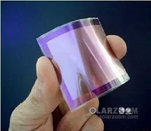
Nanocrystalline chemical solar cells (NPC cells for short) are formed by modifying and assembling semiconductor materials with a forbidden band to another large band gap semiconductor material. The narrow band gap semiconductor materials use organic compounds such as transition metals Ru and Os. The sensitizing dye and the large energy gap semiconductor material are nano-polycrystalline TiO2 and made into electrodes. In addition, NPC batteries also use appropriate redox electrolytes.
The working principle of nanocrystalline TiO2: the dye molecule absorbs sunlight and transitions to an excited state. The excited state is unstable. The electrons are quickly injected into the adjacent conduction band of TiO2. The electrons lost in the dye are quickly compensated from the electrolyte and enter the conduction band of TiO2. The electricity in the medium finally enters the conductive film, and then generates a photocurrent through the external circuit.
The advantages of nanocrystalline TiO2 solar cells are its low cost, simple process and stable performance. The photoelectric efficiency is stable above 10%, and the production cost is only 1/5-1/10 of that of silicon solar cells. The life span can reach more than 20 years.
Perovskite solar cell
In 2015, Japanese, Chinese, and Swiss researchers used thin film doping technology to create a perovskite solar cell with an area of ​​1 square centimeter, with a notarization efficiency of 15%. The researchers gave the inorganic interface layer of the perovskite cell The nickel oxide film is heavily doped with lithium and magnesium, which increases its conductivity by about 10 times.
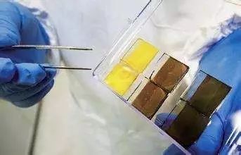
Perovskite-type solar cells are solar cells that use perovskite-type organic metal halide semiconductors as light-absorbing materials, that is, the dyes in the dye-sensitized solar cells are replaced accordingly.
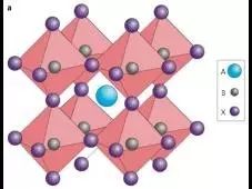
As shown in the figure, the perovskite solar cell is composed of glass, FTO, electron transport layer (ETM), perovskite photosensitive layer, hole transport layer (HTM) and metal electrode from top to bottom.
Among them, the electron transport layer is generally dense TiO2 nanoparticles to prevent the carriers in the perovskite layer from recombining with the carriers in the FTO. The conductivity of the layer can be improved by adjusting the morphology of TiO2, element doping or using other n-type semiconductor materials such as ZnO to improve the performance of the battery.
The picture below shows the structure of perovskite solar cells and their carrier transport mechanism
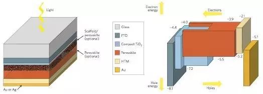
Physical processes in perovskite solar cells
When receiving sunlight, the perovskite layer first absorbs photons to generate electron-hole pairs. Due to the difference in the binding energy of excitons in perovskite materials, these carriers either become free carriers or form excitons. Moreover, because these perovskite materials tend to have lower carrier recombination probability and higher carrier mobility, the carrier's diffusion distance and lifetime are longer. This is the source of the excellent performance of perovskite solar cells.
Then, these uncomplexed electrons and holes are collected separately from the electron transport layer and the hole transport layer, that is, the electrons are transported from the perovskite layer to the electron transport layer such as TiO2, and finally collected by FTO; the holes are transported from the perovskite layer to the void. The hole transport layer is finally collected by the metal electrode.
Of course, these processes are always accompanied by some loss of carriers, such as the reversible recombination of electrons in the electron transport layer and holes in the perovskite layer, and the recombination of electrons in the electron transport layer and holes in the hole transport layer (calcium The case where the titanium ore layer is not dense), the recombination of the electrons in the perovskite layer and the holes in the hole transport layer. To improve the overall performance of the battery, the loss of these carriers should be minimized. Finally, the photocurrent is generated through the circuit connecting the FTO and the metal electrode.
Thin film solar cell
Thin-film solar cells are defined according to their thickness characteristics. Silicon solar cells have a light-absorbing layer of about 350 microns, but the light-absorbing layer of thin-film solar cells is only 1 micron thick.
The producers of thin-film solar cells have begun to reduce the number of layers of light-absorbing materials, such as semiconductors on the substrate and coated glass. The materials used as semiconductors do not need to be thick because they absorb solar energy very efficiently. Therefore, thin-film solar cells are light, durable and simple.
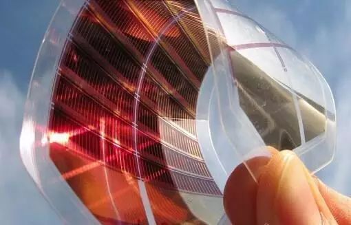
According to the type of semiconductor used, thin-film solar cells mainly fall into the following three categories: amorphous silicon, cadmium telluride and copper indium gallium selenide.
Amorphous silicon is an improved version of traditional silicon crystalline solar cells. They are widely used in solar electronic devices, but amorphous silicon also has some shortcomings and deficiencies.
One of the biggest problems of amorphous silicon solar cells is the materials used in their semiconductors. Silicon is not easy to find on the market, and supply is often less than demand; the efficiency of amorphous silicon is not high enough. Therefore, this battery is experiencing a significant decline.
Thinner amorphous silicon cells overcome this shortcoming, but the cells with reduced thickness have lower efficiency in absorbing light energy. Amorphous silicon cells are suitable for small-sized devices, such as calculators, but not for large-sized devices, such as buildings powered by solar energy.
The good development of silicon-free thin-film optoelectronic technology has begun to overcome the problems of amorphous silicon, such as cadmium telluride batteries and copper indium gallium selenide batteries.
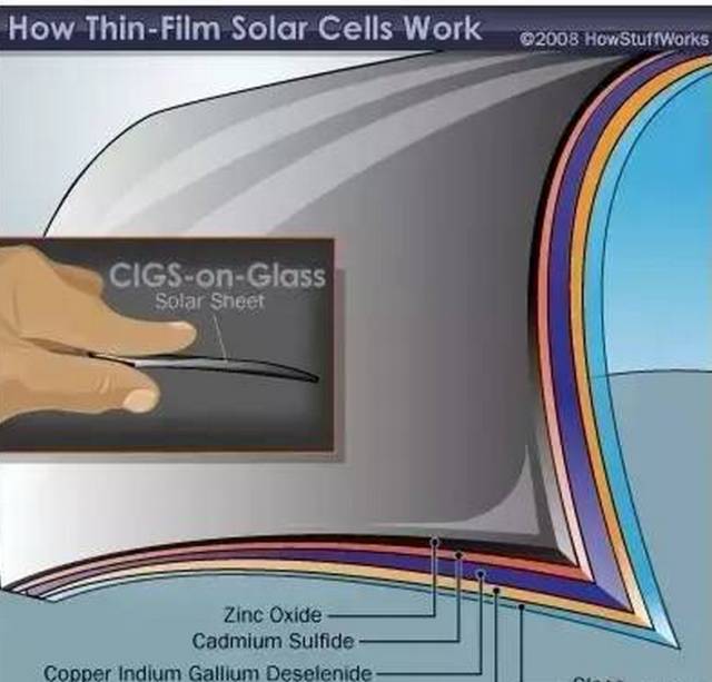
Glass-based copper indium gallium selenium solar cell
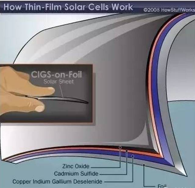
Chaff-based copper indium gallium selenium solar cell
The basic scientific knowledge behind thin-film solar cells is the same as that of traditional silicon crystal cells. Photoelectric conversion cells need to rely on semiconductors. Semiconductors are insulators when they exist as pure substances, but they can conduct electricity when heated or combined with other materials. When the semiconductor material is mixed or doped with phosphorus, there are additional free electrons, which is what we know as N-type semiconductors. When the semiconductor is doped with other materials (such as boron), there are extra vacancies that can receive electrons, which is a P-type semiconductor.
Thin-film solar cells connect N-type semiconductors and P-type semiconductors through a layer of film, which is the connection surface. Even in the absence of light, a small amount of electrons can pass through the connection surface from the N-type semiconductor to the P-type semiconductor, generating a small voltage. In the presence of light, photons can knock out a large number of electrons, and these electrons flow through the connection surface to form an electric current.
Traditional solar cells add silicon to P-type semiconductors and N-type semiconductors, while the latest generation of thin-film solar cells use thin layers of cadmium telluride or copper indium gallium selenide instead of silicon. In the form of nanoparticles, the four elements of copper, indium, gallium, and selenium are self-assembled in a uniform distribution system to ensure that the ratio of these four elements is always correct.
There are two basic shapes of copper indium gallium selenide solar cells. A glassy battery requires molybdenum to make a positive electrode, but a thin layer of molybdenum is not required in a chaff battery because the chaff can be used as an electrode. The zinc oxide film plays the role of another electrode in the copper indium gallium selenide battery. Inserted between the positive and negative electrodes are semiconductor materials and cadmium sulfide. These two thin layers play the roles of N-type semiconductor and P-type semiconductor, and are used to pass the current generated between the electrodes.
The cadmium telluride battery and the copper indium gallium selenide battery have a similar structure. One of its electrodes is made of a layer of carbon glue impregnated with copper, and the other is made of tin oxide or cadmium stannate. The semiconductor used is cadmium telluride, which together with cadmium sulfide plays the role of N-type semiconductor and P-type semiconductor.
The future development direction of solar cells
Thin-film solar cells are the most promising next-generation solar cell technology, which saves the use of silicon raw materials and silicon wafer manufacturing processes. Compared with the current common silicon wafer solar cells, silicon thin-film solar cells use only 1% of the silicon used in the former. %, the cost of solar cells per watt can be reduced from US$2.5 to US$1.2. In addition, this new high-tech product can be integrated with building roofs and wall materials such as glass curtain walls, which can be connected to the grid for power generation and save Building materials, beautify the environment.
The third-generation concentrating solar (CPV) power generation method is gradually becoming the focus of the solar field. Photovoltaic power generation has experienced the first generation of crystalline silicon cells and the second generation of thin-film cells, and the current industrialization process is gradually turning to efficient CPV system power generation.
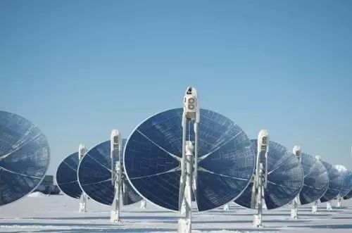
Compared with the previous two generations of batteries, CPV uses a multi-junction III-V compound battery, which has the advantages of large spectral absorption and high conversion efficiency. Moreover, the battery area required is not large, and relatively cheap concentrators are used to replace expensive semiconductor materials, which can effectively reduce costs and reduce production energy consumption when used in large-scale power generation.
As a long-lasting, universal, and huge energy source, solar energy can be said to be inexhaustible. Compared with other energy sources, the use of solar energy is clean and pollution-free, and the use of solar energy will not pollute the ecological environment. When mankind is facing energy and environmental crisis, it is urgent to find a clean, efficient and relatively sufficient energy situation to meet the social and economic development, and solar energy is one of the best choices.
The current development method of solar energy is mainly the situation of solar cells. After just a few decades of development, solar cells have been equipped with fairly mature technology and are used in all aspects of people's production and life. I believe that with the continuous improvement of technology, solar cells Will get greater development and benefit human society.
Guangzhou Bolei Electronic Technology Co., Ltd. , https://www.nzpal.com