Select the energy and dose of antimony implantation and the corresponding well push process and meet the following requirements: 1. No dislocation/stacking fault defects after epitaxial growth; 2. Determine the oxide thickness and the energy/dose of antimony implantation and the corresponding well push The relationship between the processes; 3. The thickness of the oxide layer is different between the antimony implanted area and the non-implanted area. It can be seen from Table 1 that in the case of a pad oxide layer, a low antimony implantation energy/dose is a defect-free condition, and as the antimony implantation energy/dose becomes higher and higher, dislocation/stacking fault defects become more and more. Serious (see Figure 1).
We have done relevant research on the relationship between oxide thickness and antimony implantation energy/dose and implantation/non-implantation area (see Table 2). We noticed that under the same push well condition, the closer the silicon damage to the surface, the more severe the silicon damage will result in a thicker oxide layer. This also means that we must fully consider this in the subsequent oxide layer removal process.
Another point that needs to be mentioned is that in order to avoid cross-contamination of antimony and phosphorus, the measure we have taken here is to appoint a machine to be responsible for the antimony trapping process. Lithography alignment and OVL after silicon epitaxial growth. Since the epitaxial growth is completed, the next thing we have to do is N/P well lithography, and the front layers aligned by these two lithography are all before epitaxial growth. Zero floor. But is the epitaxially grown zero-layer pattern still in good shape enough for our lithography machine to easily recognize it? the answer is negative! Due to the thicker epitaxy and the characteristics of the epitaxy process, the pattern of the front layer will more or less deform or shift during the epitaxial growth process, which brings difficulties to the subsequent photolithography alignment.
With the rise of liquid crystal panels and larger and larger sizes, high-voltage LCD drivers have increasingly attracted the attention of the market, but the high-voltage (above 40V) process is basically a blank in China. This article focuses on the main problems and key processes faced by the 40V high-voltage process platform: antimony implantation, photolithography alignment after epitaxial growth, and non-metal silicide contact holes. In addition, due to cost control and the assurance of considerable market competitiveness, the number of mask layers developed by this set of processes is quite small, only 16 layers, which brings great complexity and difficulty to the adjustment of the device, often "One shot moves the whole body", the adjustment of a device often affects several devices at the same time, and one loses the other. And we also have to face the problem of yield. Our goal is to achieve a yield of more than 90%. Based on the above considerations, we focused our main energy on the development of these key processes and the adjustment of the devices, and finally passed all the verifications and achieved a 99% yield. The following will explain in detail through the experimental process and related data.
Antimony injectionUnder the condition that the device can work normally and there is a certain process window, select the energy and dose of antimony implantation and the corresponding push well process and meet the following requirements:
1. There is no dislocation/stacking fault defect after epitaxial growth;
2. Clarify the relationship between the thickness of the oxide layer and the energy/dose of antimony implantation and the corresponding well push process;
3. The thickness of the oxide layer is different between the antimony implanted area and the non-implanted area.
It can be seen from Table 1 that in the case of a pad oxide layer, a low antimony implantation energy/dose is a defect-free condition, and as the antimony implantation energy/dose becomes higher and higher, dislocation/stacking fault defects become more and more. Serious (see Figure 1). We have done relevant research on the relationship between oxide layer thickness and antimony implant energy/dose and implant/non-implantation area (see Table 2). We noticed that under the same push well condition, the closer the silicon damage to the surface, the more severe the silicon damage will result in a thicker oxide layer. This also means that we must fully consider this in the subsequent oxide layer removal process. Another point that needs to be mentioned is that in order to avoid cross-contamination of antimony and phosphorus, the measure we have taken here is to appoint a machine to be responsible for the antimony trapping process.
Lithography alignment and OVL after silicon epitaxial growthSince after the epitaxial growth is completed, what we are going to do next is N/P well lithography, and the front layer aligned by the two lithography is the zero layer before the epitaxial growth. But is the epitaxially grown zero-layer pattern still in good shape enough for our lithography machine to easily recognize it? the answer is negative! Due to the thicker epitaxy and the characteristics of the epitaxy process, the pattern of the front layer will more or less deform or shift during the epitaxial growth process, which brings difficulties to the subsequent photolithography alignment.
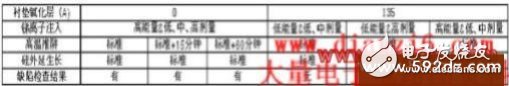
Table 1: The relationship between antimony implantation and defects with different energy and dose
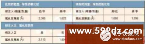
The table shows the relationship between the thickness of the oxide layer and the antimony implantation energy/dose and implantation/non-implantation area.
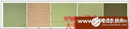
Figure 1: Defect optical comparison under different antimony implant energy/dose
In order to solve the above problems and ensure the normal alignment of the lithography machine and a fairly accurate OVL, we conducted a lot of experiments with the lithography department on the selection of LSA/FIA alignment patterns and got good results:
First consider coarse alignment. Comparing Figure 2 (a) and (b), it is obvious that we can see that the coarse alignment signal map of the LSA dark map (b) is better, and it is easier for the lithography machine to coarsely align. Next consider fine alignment. Comparing Figure 3 (a) and (b), we can see that the fine alignment signal of FIA dark image (b) is better, and it is easier for the lithography machine to fine align.
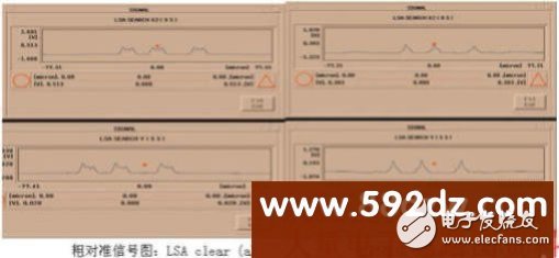
Figure 2: Signal diagrams of different coarse alignment patterns of the lithography machine
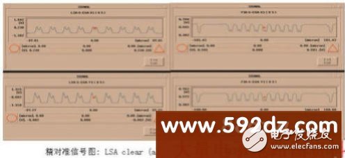
Figure 3: Signal diagram of different precision alignment patterns of lithography machine
After confirming the rough alignment and fine alignment signals of the lithography machine, we need to further confirm the corresponding fine alignment random factors and the overlay results of the lithography machine. It can be seen from Table 3 that the random factor and OVL results of LSA are quite poor regardless of clear or dark; while for FIA, the random factor and OVL results are quite good regardless of whether it is clear or dark. In addition, as to whether Global EGA can be further improved by choosing fewer points, there does not seem to be much difference from the data.
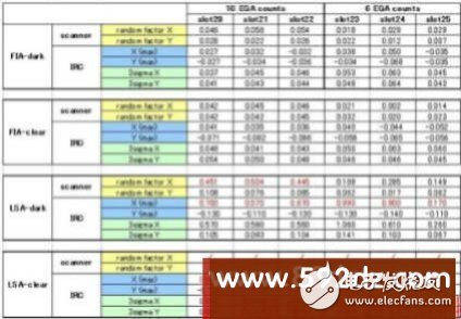
Table 3: The relationship between different fine alignment patterns and random factor/Overlay
Non-metal silicide contact holeDue to the use of non-metal silicide contact holes, although the theoretical contact resistance is higher than that of metal silicide, since we are using this process for the first time, there is no benchmark to refer to. It turns out that our process PDIFF_CT index greatly exceeds The specifications (see Figure 4).
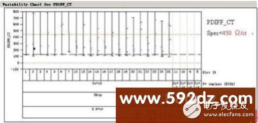
Figure 4: PDIFF_CT WAT value of non-metallic silicide
After TEM FA, we found that the step coverage of Ti/TIN at the bottom of the contact hole is quite poor (Figure 5). When we use the metal silicide process, because there is already a layer of TISi2 at the bottom of the contact hole, this effect is not too great. However, once non-metal silicide contact holes are used, such poor bottom step coverage is fatal.
Mutual influence and mutual restraint. Figure 8: 40V high voltage PMOS device structure diagram So what should we do to achieve it? Let us first understand the device structure of the 40V high-voltage device. As shown in Figure 8, our 40V high-voltage device uses an LDMOS structure, and the source/drain OFFSET is formed by a well. There is a drift zone oxide layer between the gate polysilicon and the source/drain. As far as PMOS is concerned, the entire PMOS is separated by NBL (N-Buried Layer) and N-well. In order to increase the BV, we must first know that the BV of the device depends on the source/drain punch through (Punch Through) or a certain PN junction. In fact, after we have done a lot of experiments, we found that 40V PMOS BV depends on the BV of the P-well of the drain to the NBL junction. Therefore, our goal is how to increase the BV of this junction. In order to achieve this goal, we can have two methods: 1. Reduce the concentration of NBL and P trap. But it should be noted here that if the P-well concentration is too low, Ion will be correspondingly reduced due to the increase in Rs and the shallower junction. On the other hand, if the NBL concentration is too low, it may cause the middle N-well to fail to connect to the NBL, resulting in the HVPMOS not working at all. 2. Increase the thickness of the epitaxial layer (EPI). Epitaxial thickening can not only significantly increase HVPMOS BV, but also due to the increase in junction depth, Ion can also be increased accordingly. Although the epitaxial thickening may also cause the middle N well to be connected to the NBL
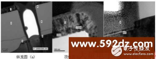
Figure 5: Contact hole TI/TIN step coverage map
After knowing the cause of the failure, after detailed discussion and careful study, we adjusted the Ti/TiN metal deposition and contact hole etching process to obtain the morphology of Figure 6. It can be seen that the step coverage at the bottom of the contact hole has been significantly improved. The improvement of this morphology has been verified on the data of WAT PDIFF_CT (Figure 7). After the improvement of the process, PDIFF_CT has dropped from more than 450 to less than 100, and the in-plane uniformity of the silicon wafer is quite good.

Figure 6: Ti/TiN step coverage diagram of contact hole after improvement
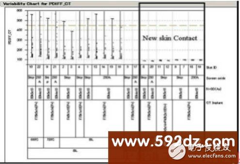
Figure 7: New structure contact hole PDIFF_CT WAT value
Device adjustmentAfter the above new process development is basically solved, our next focus is the adjustment of the device. Since the mask used for the 40V high voltage is very small, an ion implantation layer often affects several devices at the same time or the adjustment of a device often depends on several ion implantation. Although this makes our work more complicated, it is not the most difficult problem. The biggest problem we face is how to increase the breakdown voltage (BV) and operating current (Ion) of 40V high-voltage devices as much as possible at the same time. As we all know, these two parameters often influence and contain each other.
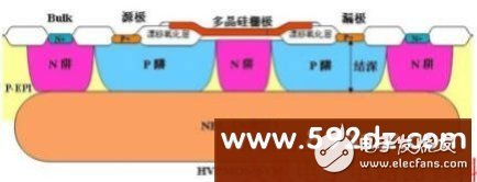
Figure 8: 40V high voltage PMOS device structure diagram
So what can we do to achieve it? Let us first understand the device structure of the 40V high-voltage device. As shown in Figure 8, our 40V high-voltage device uses an LDMOS structure, and the source/drain OFFSET is formed by a well. There is a drift zone oxide layer between the gate polysilicon and the source/drain. As far as PMOS is concerned, the entire PMOS is separated by NBL (N-Buried Layer) and N-well. In order to increase the BV, we must first know that the BV of the device depends on the source/drain punch through (Punch Through) or a certain PN junction. In fact, after we have done a lot of experiments, we found that 40V PMOS BV depends on the BV of the P-well of the drain to the NBL junction. Therefore, our goal is how to increase the BV of this junction. In order to achieve this goal, we can do two things:
1. Reduce the concentration of NBL and P well. But it should be noted here that if the P-well concentration is too low, Ion will be correspondingly reduced due to the increase in Rs and the shallower junction. On the other hand, if the NBL concentration is too low, it may cause the middle N-well to fail to connect to the NBL, resulting in the HVPMOS not working at all.
2. Increase the thickness of the epitaxial layer (EPI). Epitaxial thickening can not only significantly increase HVPMOS BV, but also due to the increase in junction depth, Ion can also be increased accordingly. Although the thickening of the epitaxy may also cause the middle N-well to fail to connect to the NBL, as long as we control it within a certain range, this problem can be avoided.
Comparing the above two methods, since the latter is more effective in increasing BV and at the same time it can also increase Ion, we choose to increase the epitaxial thickness. But here we need to remind again that the extension should not be too thick, otherwise HVPMOS will not work at all. Although we indirectly increased Ion by increasing the epitaxial thickness, there is still a certain distance from our goal. Therefore, we have to further improve from another angle.
Note that there is a drift oxide layer between the gate polysilicon and the source/drain. If we can reduce the P-well Rs under the drift oxide layer, Ion can be further improved. Following this line of thinking, we can add a boron (Boron) implant to reduce Rs before the field oxide grows. In fact, we did exactly this, and indeed further improved the 40V PMOS Ion. But there are also two points to note here:
1. This boron implantation increases the concentration of the P-well, so this may reduce the BV of HVPMOS, which needs to be weighed and considered;
2. This time the boron implantation will also be implanted into the N-well region, so this will increase the Rs of the N-well, thereby reducing the 40V NMOS Ion, which also needs to be considered.
Yield improvementAfter the process and device problems are basically solved, what we have to do further is to confirm what our yield rate is and how it should be improved. Let's look at the benchmark yield first. From the yield bin map in Figure 9, we can see that the yield varies from 25% to 94%, and the main reason is that Bin8 and Bin13 fail. In addition, we summarized the relationship between yield rate and WAT, and found that yield rate has a strong relationship with 5VNMOS Vt. It can be seen from Fig. 10 that with the increase of 5VNMOS Vt, the yield rate is getting lower and lower. Based on the above analysis, we quickly adjusted the 5VNMOS Vt, and as a result the yield rate increased to 99% (Figure 11).
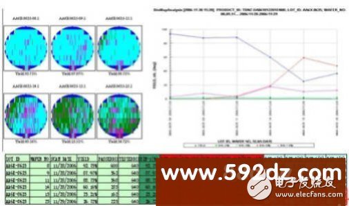
Figure 9: 40V high voltage yield and bin map
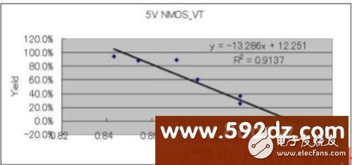
Figure 10: Negative relationship between 5VNMOS_Vt and yield
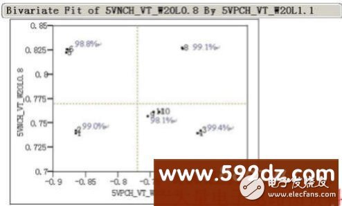
Figure 11: The relationship between the yield rate and Vt after 5VNMOS Vt adjustment
Summary of this articleIt can be seen from the above data that the development of the 40V high-voltage process platform is quite successful. This is not only reflected in the various monitoring indicators and the final WAT, but the 99% yield rate confirms this. Therefore, the successful development of the 40V high-voltage process not only fills the gap in this technology in China and improves the high-voltage product series, but also brings significant economic benefits. In addition, these key processes are not only suitable for 40V high voltage, other projects in the future can also be used for reference.
OVNS 1500 Puffs Vape is so convenient, portable, and small volume, you just need to take them
out of your pocket and take a puff, feel the cloud of smoke, and the fragrance of fruit surrounding you. It's so great.
We are the distributor of the ovns & vapeak vape brand, we sell ovns disposable vape,ovns vape kit, ovns juul compatible refillable pod, and so on.
We are also China's leading manufacturer and supplier of Disposable Vapes puff bars, disposable vape kit, e-cigarette
vape pens, and e-cigarette kit, and we specialize in disposable vapes, e-cigarette vape pens, e-cigarette kits, etc.
ovns 1500 puffs vape bars,ovns 1500 puffs vape device,ovns 1500 puffs vape disposable,ovns 1500 puffs vape starter kit,ovns 1500 puffs vape pen
Ningbo Autrends International Trade Co.,Ltd. , https://www.ecigarettevapepods.com