OLED inkjet printing
Mainly using solvents to melt OLED organic materials
Then the material is directly printed on the surface of the substrate to form an R (red), G (green), B (blue) organic light-emitting layer.
What I prepared for everyone today is
Analysis of materials in the process of inkjet printing, as well as its processes and difficulties
Inkjet printing polymer material
Due to the large molecular weight of the polymer, it is mainly processed into a film by solution, such as spin coating or printing, and ink jet printing technology has proven to be the best method for preparing a luminescent polymer solution. In 1990, Richard Friends and others discovered the electroluminescence properties of polymers at the Cavendish Laboratory of the University of Cambridge and produced polymer light-emitting diodes (PLEDs). Since then, the PLED display has attracted great attention and is considered to be Most promising for the next generation of flat panel displays.
In 1998, Hebner et al. first used inkjet printing technology to prepare doped polymer light-emitting films and PLED displays.
In the same year, Bharathan and Yang used inkjet printing of water-soluble conductive ink PEDOT using Epson desktop printing equipment to prepare a monochrome PLED electronic label.
In 1999, they successfully prepared a two-color PLED display using both spin-on and ink-jet printing processes, and showed the first full-color PLED display made using inkjet printing technology on the US SID. Since then, The United States Dupont Display Company and many other research and development institutions have developed their own full-color PLED displays using inkjet printing technology.
In 2000, Kodayashi et al. [22] used Epson equipment to print red and green luminescent polymer materials on a substrate coated with an electron transport material polydioctyl fluorene (F8) - a styrene-supported (PPV) solution. They successfully printed the luminescent material onto the thin film transistor and displayed red, green, and blue color images.
In 2002, Duineveld et al. reported a true color 80 ppi active (AM-PLED) and passive PM-PLED display based on inkjet printing.
In 2004, SeikoEpson used a splicing technique to make an inkjet printed full-color PLED display with a diagonal of 102 cm, a thickness of only 2.1 mm and a life of 2000 h or more.
In 2010, Singh et al. produced an OLED display based on inkjet printing technology. The luminescent material is a macromolecular phosphorescent dye containing germanium atoms, the hole transporting material is poly(9-vinylcarbazole), and the electron transporting material is PBD. Their inkjet print display has a maximum luminous brightness of 6000 cdm-2, a low switching voltage of 6.8 V (5 cd·m-2), and a relatively high quantum efficiency of 1.4%. By improving the chemical structure of the dye and the morphology of the printed film, they obtained the result of a maximum luminance of 10,000 cd·m-2.
In recent years, people have made great efforts to improve the pixel resolution, film uniformity and longevity of the display screen. The research on inkjet printing deposited optoelectronic materials has become more and more active, and it has proved the hole transmission of the display screen. Layers, luminescent layers, and cathode materials can all be fabricated using inkjet printing technology, laying the groundwork for a fully printed display.
Although high-efficiency, printable polymer luminescent materials have been greatly developed, inkjet printing equipment and related film-forming processes can basically meet the requirements for preparing high-resolution displays. However, the performance of luminescent polymers still needs Researchers continue to work to develop polymer materials that are more luminous, longer lasting, and less expensive to meet growing market demands.
Inkjet printing of small molecular materials
At present, the efficiency of polymer light-emitting devices (PLEDs) (6-8 cd/A) and lifetime are generally low, while small-molecular light-emitting devices (SM-OLED) have obvious performance advantages, such as high efficiency (84 cd/A) and long Life expectancy, etc. PLEDs still have limitations in their applications, and multilayer phosphorescent small molecule light-emitting display devices (SM-OLEDs) processed by thermal evaporation processes can achieve higher efficiencies.
Xia et al. used these traditional hot-vapor deposition small molecular materials to make thin films by inkjet printing, and prepared phosphorescent small molecule light-emitting devices with better performance. The research on inkjet printing small molecules has caused more people. s concern.
Obtaining high quality functional films is essential for making high efficiency, long life devices. However, the general small molecular material has poor film-forming property, and the liquid film is prone to dewetting to form a discontinuous film during drying on the substrate. Therefore, the film formation of the small molecule itself can be improved by two ways. . One is to increase the molecular volume and alkyl chain length, and to design molecules with good solubility and film formation; the second is to add polymer materials to small molecular materials to improve film formation.
In addition, changing the physicochemical properties of the substrate surface can also improve the film formation of the material. Sirringhaus et al. inkjet printed a water soluble material on the surface of a hydrophobic substrate patterned with a hydrophobic material to obtain a high resolution polymer electrode.
Hendriks et al. printed a nano-silver ink wire on the surface of a thermo-embossed substrate. When the contact angle is small, the ink is sucked into the channel by capillary action. Because the fluid properties of small molecule solutions depend mainly on the nature of the solvent, although the effect of solvents on the film formation of small molecules has been extensively studied, the effect of solvents on the film formation of small molecules is very complicated.
Inkjet printing cathode
As with the principle of vapor deposition of small molecules, the cathode of an OLED device is also generally produced by a vacuum evaporation process, and the vapor deposition apparatus and the mask used are relatively expensive.
The use of inkjet printing technology to prepare the cathode can greatly reduce the cost, and the biggest problem is uniform film formation over a large area.
In the research of all-printing process for preparing OLED displays, the key is the development of printable cathode inks and the realization of large-area film-forming technology. The difficulty lies mainly in:
1
The affinity of the cathode material to the organic functional layer must be ensured to ensure stable film formation of the printed cathode;
2
The fineness of the printed pattern must be guaranteed to ensure the high resolution of the displayed image;
3
Damage to the underlying layer of the cathode cement must be avoided;
4
Effective injection of carriers must be guaranteed to ensure high brightness and high efficiency display performance.
Inkjet printing OLED display process
When inkjet printing functional film, the droplet pitch (μm) and droplet volume (pl) need to achieve higher precision to meet the uniformity and thickness requirements of the film.
The droplet positioning or small changes in volume may cause the brightness of the display pixel pit to be uneven or even short-circuited, resulting in a large number of defects in the OLED display.
The OLED functional layer not only requires uniform film thickness, but also maintains its own photoelectric characteristics, so the solvent must be dried and removed during film formation;
Also, other additives in the ink must be removed to the lowest level to avoid affecting the performance of the organic semiconductor film.
Therefore, the development of inkjet printing to prepare OLED display technology not only drives the development of inkjet printers/printers, but also attracts people's attention and in-depth research on ink formulation, ink/substrate interface contact characteristics and drying process.
Pixel pit size and calculation of inkjet print droplets
The OLED display panel is composed of a pixel array, and each pixel is composed of sub-pixel pits of three colors of red, green and blue. Generally, the geometric shape is a rounded rectangle as shown in the following figure.


The size and number of pixel pits are determined by the application characteristics of the display:
For high-definition televisions (HDTVs), the sub-pixel pits are 140 and 250 μm in size with a pixel array of 1080×1920 and a size of 94 to 165 cm. For mobile devices such as smartphones, the pixels are wide video images. The array (WVGA, 480 × 800 pixels), sub-pixel pit size is 26 μm and 35 μm, respectively, in the specifications of 7.37 to 9.65 cm.
Since the color of the sub-pixel pit luminescent material adjacent to the color display screen is different, it is necessary to prevent the solution from overflowing into the adjacent pixel pit during printing, so it is necessary to create an isolation region with low surface energy between the pixel pits, generally using a photoresist. Resin is used as the insulation material.
When printing ink into a pixel pit, first consider whether the ink volume meets the thickness requirements of the film.
Since the area and depth of the pixel pit are constant, the ink volume must be filled with pixel pits and cannot overflow the pixel pit, so the volume of the printing ink is limited.
Assuming that the ink having a concentration of 1% (mass fraction) is printed into the pixel pit, the film thickness is required to be 70 nm.
The maximum volume of the small pixel pit is smaller than the ink volume that satisfies the thickness requirement (the liquid-substrate contact angle is 70°), that is, the maximum film thickness after the ink fills the pixel pit is still less than 70 nm, indicating that the solid content in the ink is too low, and the ink needs to be increased. Concentration and reduce printing volume.
The ink volume required to reach a film thickness of 70 nm in a large pixel pit is smaller than the minimum wetting volume (the contact angle of the ink to the substrate is 15°), that is, the ink is insufficient to cover the pixel pit, indicating that the solid content in the ink is too high, and the ink needs to be lowered. The concentration and increase the volume of the printing ink.
In the case where both the ink concentration and the droplet volume are determined, the ink volume and the number of ink droplets required for each pixel pit can be calculated according to the film thickness requirement. Since the droplet volume is determined by the diameter of the print head, the print head of the corresponding diameter can be selected according to the size of the pixel pit. The smaller the pixel pit size, the smaller the diameter of the selected print head, and the higher the technical requirement.
Ink film formation process control
The solution of the inkjet printed OLED display is mainly composed of a photoelectric material and a solvent, and it is necessary to consider the formulation of the ink from the characteristics of the fluid, the degree of spreading, and the drying process:
1
To ensure the stability of the ink, it is required to have a high solubility or uniform dispersion of the solute, to ensure the stability of the droplets and to form a uniform film on the substrate;
2
The rheology (viscosity, surface tension and shear rate) of the solution must meet the requirements of inkjet printing equipment, and can form stable droplets, including droplets without satellite points, good repeatability, accurate positioning, etc.
3
The solvent does not evaporate too quickly, preventing the dried solute from clogging the printhead and causing printing failure.
The printability of ink is primarily determined by the amount of change in viscosity, surface tension, and shear rate, while molecular structure and molecular weight, solids content, and solvent selection are the primary factors affecting these physical parameters.
Inkjet printing equipment generally requires ink viscosity between 1 and 20 cP.
For polymer inks, the higher the solute content, the greater the viscosity of the ink, and the solid content is generally between 0.2% and 2.5% (mass fraction);
For small molecules, the solute content has little effect on the viscosity of the solution. Generally, the viscosity of the solution is increased by selecting a high viscosity solvent and adding an additive. The boiling point and surface tension of the solvent determine the drying rate of the ink and the wetting of the substrate. Sex, so it is necessary to select a solvent with appropriate physical properties to achieve the purpose of controlling the film formation morphology of the solute in the pixel pit.
The ideal situation for ink to spread in a pixel pit is:
The contact angle between the liquid and the pixel pit substrate is small, and the contact angle with the pixel edge is large to ensure that the liquid does not overflow within the pixel pit.
This wetting property is obtained by processing the surface of a pixel substrate (such as ITO) and its edge material (such as PI), including the structure of the modified substrate material, the process of making the substrate, and surface treatment (such as plasma, ozone or solution treatment). Wait).
After the droplets are covered with pixel pits, the dry film formation process can be explained by the "coffee ring" effect proposed by Deegan et al.
When the droplet spreads on the substrate, surface defects and other causes cause the solute to “pin†at the contact line, and the droplet will continue to maintain the spread shape. Since the solvent volatilizes at the contact line, the solution will flow from the middle of the droplet. The solvent is transferred to the edge of the droplet to compensate for the volatilized solvent, and the final solute is deposited on the substrate to form an uneven film having a thin intermediate thickness, that is, a "coffee ring."
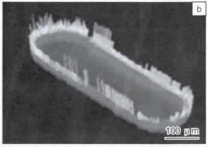
By adding a high boiling solvent, the evaporation rate of the solvent at the contact line can be reduced, and an inward Marangoni flow can be formed to uniformly deposit the solute. The above figure b is a photograph of a three-dimensional pixel pit interfered by white light, and it can be seen from the uniform color that the ink forms a film having a uniform thickness.
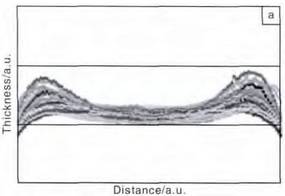
A white light interferometer can be used to measure the film thickness profile along a certain direction (long axis or short axis direction) of the pixel pit. The following two figures are the thickness distribution of the PEDOT:PSS ink dried film in a pixel pit in a certain direction. Figure a is the result of inkjet printing a single solvent ink. The film is uniform in the middle and the edges are raised to form a coffee ring structure.

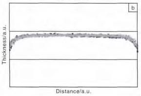
In order to suppress the uneven deposition of this solute, the reconstituted PEDOT:PSS ink (adding high boiling point solvent) was ink-jet printed, and the drying time of the edge ink became longer, eventually forming a uniform distribution curve of the film thickness shown in the following figure b. .

Droplet positioning deviation and control
Important technical specifications for inkjet printers/printheads include the positioning accuracy of droplets, inkjet droplet volume, print reliability and yield.
The target position of the drop is determined by the geometric pattern of the display, which is primarily determined by the diameter of the printhead.
Since the pixel size of the display screen is generally on the order of micrometers, the higher the resolution, the smaller the volume of the droplet and the more accurate the positioning. For example, in a pixel resolution of 100-150 ppi (sub-pixel size is about 85-55 μm), a color display substrate of 35.56 cm is deposited with 1 to 20 million droplets having a diameter of about 25 μm, and the droplet positioning is slightly deviated, which may cause The printing of the entire pixel substrate is wrong, so the size of the print head is required to be about 10 pl, and the drop drop accuracy is within ±10 μm, so that a device with accurate printing positioning and high resolution can be obtained.
The drop position deviation is primarily caused by the mechanical offset of the print platform and the offset angle of the drop at the exit of the printhead. Equipment used in the manufacture of inkjet printed displays typically have a professional high-precision printing platform (such as an air bearing platform) that meets the requirements for mechanical displacement accuracy.
The offset angle of the droplet at the exit of the printhead is affected by the design of the printhead and the formulation of the ink, because the printheads used to produce the display are specially designed to have an impact on droplet deflection. Small, the droplet offset angle is generally not more than 10mrad.
Through the design of the print head and the optimization of the ink, the droplet deflection angle can reach ±2mrad, and the corresponding printing resolution can reach 200ppi.
In addition, by optimizing the chemical composition of the ink, regulating the chemical composition or physical structure of the substrate surface, the size of the ejected ink droplets can be reduced or the spreading wettability of the ink droplets on the surface of the substrate can be controlled, and the inkjet printing can be effectively improved. Resolution.
These methods of increasing print resolution are very important in making OLED displays.
Substrate structure design
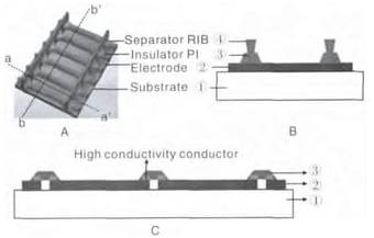
The figure below is a structural diagram of a conventional passive organic light emitting display (PM-OLED) substrate (Fig. A, B) and a modified substrate (Fig. C). The substrate is formed by laminating a transparent substrate 1, an electrode 2, an insulating layer PI3, and a spacer RIB4 in this order (FIG. A).

Although the substrate structure solves the high cost problem of using the evaporation mask, the substrate is used for the full solution processing technology to prepare the display screen to face the following three problems:
1
The isolation column RIB4 affects the quality of the functional film;
2
The unevenness of the functional film is liable to cause breakage of the cathode or the occurrence of pores, resulting in an open circuit or short circuit of the display screen;
3
The electrode 2 is etched into strips, which increases the resistance of the transparent electrode, which is easy to cause difficulty in current injection of the device and decrease in current density of the display screen, resulting in an increase in the display driving voltage, and a decrease in luminance and luminous efficiency.
Zheng et al. designed a new type of dot matrix display substrate suitable for full printing:
On the basis of the conventional substrate structure (Fig. 3A, B), the isolation column RIB4 is removed, and on the substrate of the simplified non-isolation column RIB4, a fully printed organic electroluminescent dot matrix display with reduced or no defects is prepared; The width of the large electrode strip 2 (Fig. C) and the high conductivity wire (Fig. C) are introduced in the light-emitting region, and the substrate structure is optimized from these two aspects to realize high-brightness, high-efficiency, long-life, low-cost organic electroluminescence. Dot matrix display.
Anti-virus disposable safety coverall protective clothing
This product is non-sterile
It can be used in hospital, just hospital staff need to do sterilization before using;
It can effectively resist the penetration of bacteria, viruses, alcohol, blood, body fluids, air dust particles, can effectively
protect wearer from the theat of infection.
Protective Work Clothing,Ebola Protective Clothing,Safety Protective Clothing,Disposable Protective Clothing
Guangzhou HangDeng Tech Co. Ltd , http://www.hangdengtech.com