I am a longtime user and fanatic of MCUs, and I am particularly interested in multi-functional low-cost MCUs. Such MCU modules can achieve excellent communication capabilities through a single chip. I have done a lot of interesting gadgets, including: MP3 player, alarm clock, wireless ground humidity control system, pet activity monitor, Bluetooth low energy gesture control. In these small projects, the MCU realizes the collection and transmission of information and is very convenient to use.

Recently, I took over a project that not only required me to use FPGAs, but also required me to use the more powerful ARM. This is an area that I have never touched. In this series of blogs, I will introduce how I apply my existing MCU knowledge and experience to the FPGA. This article starts with the advantages and disadvantages of FPGAs and introduces the Terasic DE10 Nano development kit and the role of IP cores in FPGA design.
About FPGA
If you develop a project that has always been related to the MCU, you will certainly find that the learning curve of the MCU is not steep, the development tools used can be easily obtained, the process of development and debugging is simple, and the design is very easy to use. However, you will also find that the MCU is very limited in handling complex transactions, operating speeds, and interface diversity. The project that I personally experience has always been the ideal choice for the MCU because the functions are neither complicated nor important.
A FPGA is an integrated circuit that includes a programmable logic element (LE) whose programmable elements are already built into the chip and are very flexible. For example, they can improve system performance by programming as an accelerator or RAM, program new standards or algorithms, and add various communication interfaces as needed, all of which help reduce system costs and extend the product life cycle. . However, the disadvantage of this design is that the learning curve is very steep. For MCU developers, when learning the FPGA, it is difficult to learn because of changes in the IO port and encoding method. For an MCU, only one or a group of IOs can be flipped at the same time, and all IOs have only one voltage standard. The IO of the FPGA is processed in parallel, and the IO of different banks can follow different voltage standards.
Fortunately, I discovered the Intel Cyclone V SoC DE10 Nano development kit. The Intel Cyclone V SoC combines the FPGA with a dual-core ARM Cortex A9, allowing the FPGA to be configured in a variety of ways. The development kit includes display and communication ports, buttons and switches, pin mapping and quick configuration tools, a JTAG debugger, and Teraic and Intel. Documentation instructions and guides.
Planning FPGA Development
When planning MCU development, we first determine which interfaces are required, such as SPI, I2C, Wi-Fi, etc., and then make MCU selections based on the MCU's voltage, pin count, provided communication interfaces, supported libraries, and prices. When using an FPGA, all communication interfaces are implemented by programming, so there is no need to consider the limitations of the communication interface. The limiting factor is the number of logical units because the required ports, soft cores or memory units are all created based on these logical units. Therefore, the trade-off is that the greater the number of logic cells, the more powerful the FPGA and the higher its cost. Although FPGAs generally have high initial costs, they are not costly because they can implement the functions of multiple chip components and can also save a lot of board space.
I found myself at a critical moment: How do I determine how many logical units my design requires? The answer is that this depends on the need for IP cores, which consist of protocols, functions, code, and specific tasks performed by external modules. Almost all FPGAs consist of logic elements LE, registers, and I / O banks. Specifically:
• The logic unit LE is programmable and is a gate array inside the FPGA. Each logic unit has a certain number of lookup tables, flip-flops, and multiplexers.
• Registers are a set of triggers that can hold data and implement functions such as timers.
• I/O bank is a set of input/output pins for connecting external circuits. Each bank has an independent voltage standard, and there is a limit on the size of the current.
At first I didn't realize the importance of IP cores because I haven't yet realized the fact that IP cores have the ability to replace physical devices such as MCUs, communication controllers, or something else I would use. A chip to achieve something.
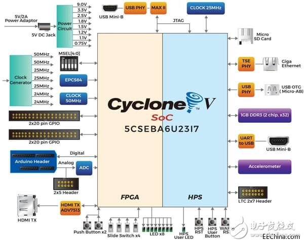
As shown in Figure 1, Cyclone V includes the FPGA layer and the HPS layer. On the DE10 Nano, the FPGA layer is mainly used as a low-latency I/O extension. All of this embodies another design feature of FPGA: it can realize the function of the chip on a plurality of PCBs on a single chip, thus, making subsequent design more flexible.

Figure 1: Interface layout for the Terasic DE10 Nano Cyclone V FPGA and Hardware Processor System (HPS). (Source: Terasic)
Most low-level I / O ports are controlled and connected through the FPGA. This reduces the time the CPU waits for low-level I / O ports. It also allows data to be processed or adjusted before being passed to the HPS.
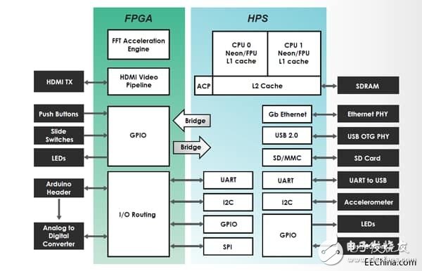
This is a perfect design. The interfaces of Cyclone V FPGAs are scalable and they can implement accelerator functions. This design architecture improves the processing capability of the HPS layer. In this case, as shown in FIG. 2 , the HDMI interface is a non-HPS local interface, so there are not many MCU resources for HDMI.

Figure 2: Interface layout of FPGA and HPS (Source: Terasic)
After a brief observation, I noticed the following advantages:
HDMI output runs on the FPGA, which reduces CPU load and adds non-local interfaces;
There is an OpenCV acceleration example, which is to show the advantages of the combination of the two types of processors;
Terasic has implemented a basic communication function paradigm and has a predefined pin-map list that defines voltage and current limits.
In general, I like FPGA very much, and I am very interested in its expansion and acceleration. However, I also want to know what limitations they have. Can they run to a high frequency? What protocols can they support? How much LE do they consume? In general, IDE is much simpler than other software I have used, and it contains amazing documentation. The hardware seems to be very powerful, and now I am designing a project that will test the board's hardware limitations.
2V Lead Acid Battery,Rechargeable Lead Acid Battery,12V 60Ah Lead Acid Battery,Lead Acid Battery For Railway
Henan Xintaihang Power Source Co.,Ltd , https://www.taihangbattery.com