Supercapacitors have significant advantages such as high power density, charge and discharge time, long cycle life and wide operating temperature range, which are suitable for applications with high power energy flow. Supercapacitance values ​​typically reach several thousand Farads, but the voltages that can be tolerated are low and must be used in large numbers in series for practical use. At the same time, the supercapacitor self-leakage rate greatly exceeds the traditional chemical energy storage components such as lithium batteries, and it is impossible to store energy for a long time. This requires that the super capacitor needs to be quickly charged before it is used for the first time or before it is put into electrical equipment for a long time. The supercapacitor maintains a certain amount of energy inside.
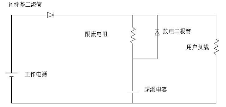
Farad capacitor charging circuit diagram (1) super capacitor charging and discharging circuitThe size of the current limiting resistor depends mainly on the power of the user's power system. If the power of the user's power system is relatively large, the current limiting resistor can be smaller. If the power of the power supply is relatively small, then the resistance is larger, and the power of the resistor is also noted. Normal power must be above 1W. For example, the maximum operating current of the power supply is 1A, and the voltage is 5V. Then the current limiting resistor takes about 5 ohms and the power is 5W. This charging circuit is limited to super capacitors with small internal resistance, such as column super capacitors. For super capacitors with large internal resistance, there is no need for current limiting resistors, such as button type super capacitors. The discharge diode can select a Zener diode with a small forward voltage drop and a certain power.
This circuit diagram is about 36VIN, 5.6A, two 2.5V series supercapacitor charger circuit connection diagram
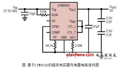
The LTM8026 is a 36VIN, 5A constant voltage, constant current (CVCC) step-down μModule® regulator. A switch controller, power switch, inductor, and support components are built into the package. The LTM8026 operates from a 6V to 36V input voltage range and supports an output voltage range of 1.2V to 24V. The CVCC operation allows the LTM8026 to accurately regulate its output current up to 5A over the entire output range. The output current can be set with a single control voltage, a single resistor or a thermistor. A complete design can be achieved with only the resistors responsible for setting the output voltage and frequency, as well as the large input and output filter capacitors.
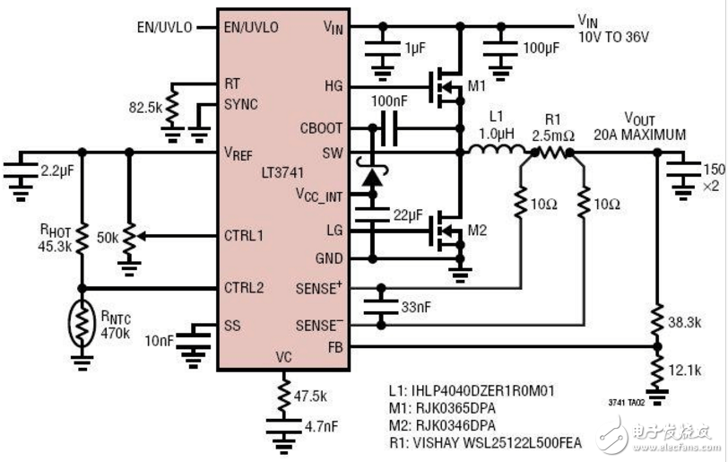
Farah capacitor charging circuit diagram (3)5V, 20A super capacitor charging circuit composed of LTR3741
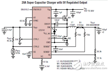
Figure LTR3741 5V regulated output 20A super capacitor charger circuit diagram
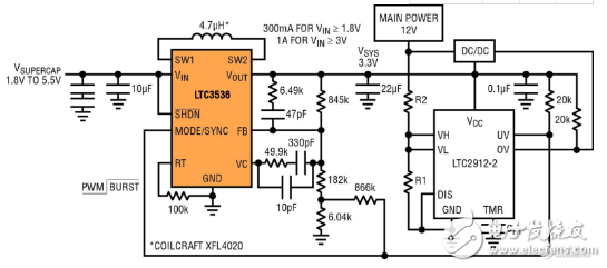
Farad capacitor charging circuit diagram (4)In this application, two series supercapacitors are charged to 5V during normal operation to provide the required backup power in the event of a main power failure. As long as the main power supply is connected, the LTC3536 will operate in a very low quiescent current Burst Mode operation, minimizing the power consumption of the backup storage capacitor.
The LT3741 is a fixed frequency, synchronous step-down DC/DC controller designed to accurately regulate output currents up to 20A. The average current mode controller will maintain inductor current regulation over a wide output voltage range of 0V to (VIN - 2V). The regulated current is set by an analog voltage on the CTRL pin and an external sense resistor. The LT3741 utilizes a unique topology to supply and sink current. The regulated voltage and overvoltage protection circuit is configured with a voltage divider connected between the output and the FB pin. The switching frequency can be set from 200kHz to 1MHz with an external resistor or with an external clock signal.
The easiest way to charge a supercapacitor through a solar cell is to use a diode. Under normal lighting conditions, even considering the losses caused by the diode, the supercapacitor can be charged to the open circuit voltage of the solar cell. Figure 1 is a schematic diagram of a supercapacitor charged with the help of a diode. Most systems require an auxiliary overvoltage protection circuit to protect the supercapacitor and subsequent load electronics.
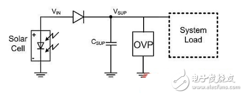
Figure 1: Schematic diagram of charging a supercapacitor using a diode
The simplicity of this solution makes it often a low-cost solar accessory. But this method has many shortcomings. First, it can only be used in multi-body solar cells, where the open circuit voltage of the solar cell is higher than the overvoltage limit of the supercapacitor or the required load voltage. Thermoelectric collectors that output low voltages cannot use this method to charge energy storage components.
In addition, the circuit regulates the solar cell at a diode drop above the storage medium voltage. This means that when the voltage on the storage medium changes according to the load conditions, the voltage regulation point of the solar cell also moves. This is not an ideal solution for a battery with a broad discharge curve or a supercapacitor whose voltage can vary significantly with load requirements, since the voltage of the solar cell is adjusted away from its maximum power point. The auxiliary overvoltage protection circuitry required in most low-power electronic systems also consumes quiescent current, which can affect system efficiency during low light periods.
Insufficient diode charging can be overcome using integrated circuits specifically designed for use with energy harvesting equipment. One such device is the bq25504. This is an ultra-low quiescent current charger IC that provides maximum power point tracking (MPPT) to the connected energy harvester. Figure 3 is a schematic diagram of how the device can be used to charge a supercapacitor. For the sake of clarity, only the necessary pins are shown. Resistors ROV1 and ROV2 are used to set the overvoltage threshold of the supercapacitor. Resistors ROK1, ROK2 and ROK3 are used to set the upper and lower thresholds of the VBAT_OK signal, which can be used to control the system load to prevent over-discharge of the supercapacitor. The solar cell is connected to the pin VIN_DC.
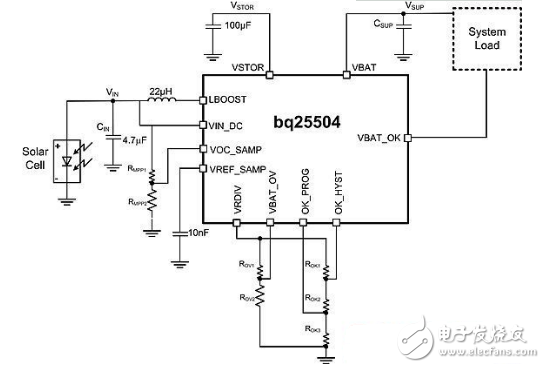
Figure 3: Schematic diagram of charging a supercapacitor using a boost charger IC
Since the supercapacitor does not collect energy input for a long time, it usually discharges to 0V, so the system needs to be started from the case where the storage capacitor is completely emptied. Most dedicated energy harvesting charger ICs have a cold-start feature that initiates charging of an energy-storing component in a fully discharged state as long as the input supply voltage is above a certain level. In this example, the voltage value is 330mV.
One of the advantages of using a boost charger IC to charge a supercapacitor is the ability to use a single or dual-body solar cell that provides a greater average power supply for the same solar cell area than a multi-body solar cell. This IC with built-in overvoltage protection circuit helps protect supercapacitors and load electronics. The user programmable VBAT_OK level can be used to signal the load circuit. Moreover, once the device enters the normal charger mode, the IC's MPPT function helps stabilize the solar cell at the maximum power point, thereby extracting the optimal power source from the solar cell.
Farah capacitor charging circuit diagram (7) fast charging road working principleFigure 1 shows the topology and control block diagram of a supercapacitor fast charging circuit based on a flyback converter. Including input rectifier bridge, flyback transformer, switching device connected in series on the primary side, secondary side freewheeling diode, current sensor, secondary side isolation voltage detection and control PWM signal generation circuit. Compared with the traditional flyback circuit, the supercapacitor fast charging circuit removes the input filter electrolytic capacitor and increases the reliability of the circuit; the current detecting resistor is changed to magnetic coupling detection to reduce the loss, and the primary side of the transformer can be simultaneously detected. And the secondary current is used to limit the secondary side charging current; the secondary side voltage isolation detection is used to control the super capacitor charging cutoff voltage. The working principle of the main circuit is basically similar to the principle of the flyback circuit, but the control circuit is designed in combination with the initial charging characteristics of the super capacitor to meet the requirements of long-term short-circuit current limiting charging when the super capacitor is initially charged.
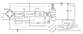
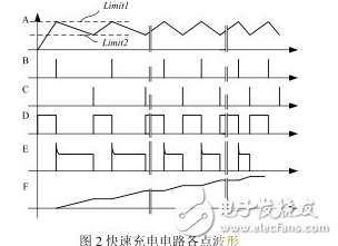
In Figure 2, A is the Current Sensor waveform. The primary current and the secondary current of the transformer are detected in the same ratio as the transformer. Since the primary side of the transformer is inversely proportional to the turns ratio, the detected current becomes a continuous current waveform. The voltage comparator (Voltage Comparator) compares the detected current value with the limit value Limit1. When the primary current value is the limit value Limit1, the signal B is generated to generate the drive signal to turn off the power tube.
Control circuitIf an electrolytic capacitor is connected to the rectified output side, a stable DC input voltage can be obtained. Since the aluminum electrolytic capacitor may have a failure problem and a life limit, the circuit stability and the working life are affected to some extent, so the input aluminum electrolytic capacitor is avoided in the fast charging circuit. The pulsating DC voltage after rectification is used as a reference for the upper limit amplitude Limit1, so that the input current follows the fluctuation of the input voltage, and the input power factor can be improved. If the lower limit amplitude Limit2 is set to 0, the power factor can be further improved, but the output current ripple amount is increased.
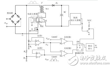
The schematic diagram of the control circuit is shown in the figure. The control circuit is composed of an operational amplifier LM358, a comparator LM393, and an RS trigger chip CD4043. The current is detected by the transformer with the same turns ratio as the transformer, and the same name end of the transformer is consistent with the flyback transformer. The current sense signal is conditioned by the LM358 and compared to the current limit values ​​Limit1 and Limit2. The output of the two comparators is latched by the flip-flop RS4043 and used as the MOSFET drive signal. The output side voltage detection is used as a charge termination signal to control the CD4043 enable terminal.
0.50Mm Pitch Series Connector,0.5Mm High Speed Board-To-Board Connectors,Double Slot Board-To-Board Connectors,Single Slot Board-To-Board Connectors
Dongguan SOLEPIN Electronics Co., Ltd , https://www.wentae.com