In a switching power supply topology with a transformer, when the switch is turned off, the loss caused by the overlap of voltage and current is the main part of the switching power supply loss. At the same time, due to the stray inductance and stray capacitance in the circuit, the power switch is off. At break, an overvoltage also occurs in the circuit and oscillates. If the spike voltage is too high, the switch will be damaged. At the same time, the presence of oscillations also increases the output ripple. In order to reduce the turn-off loss and the spike voltage, it is necessary to connect a buffer circuit at both ends of the switch to improve the performance of the circuit.
The main functions of the snubber circuit are: one is to reduce the conduction or turn-off loss; the other is to reduce the voltage or current spike; the third is to reduce dV / dt or dI / dt. Since the current of the MOSFET tube drops rapidly, its turn-off loss is small. Although the MOSFET tube still uses a shutdown snubber circuit, its function is not to reduce the turn-off loss, but to reduce the leakage inductance spike voltage of the transformer. This article focuses on the turn-off snubber circuit of the MOSFET.
1 RC snubber circuit designWhen designing an RC snubber circuit, you must be familiar with the topology of the main circuit. Figure 1 shows the snubber circuit of a forward converter consisting of RC. In the figure, when Q is turned off, the collector voltage starts to rise to 2Vdc, and the capacitance C limits the rising speed of the collector voltage, and at the same time reduces the overlap of the rising voltage and the falling current, thereby reducing the loss of the switching transistor Q. Before the next switch is turned off, C must discharge the already filled voltage 2Vdc, and the discharge path is C, Q, R.
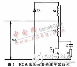
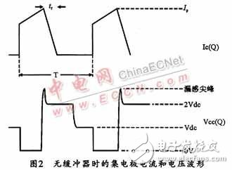
Assuming that the switching transistor has no snubber circuit, the reset winding of the forward converter shown in Figure 1 has the same number of turns as the primary winding. Thus, when Q is turned off, the energy stored in the magnetizing inductance and the leakage inductance is released, the voltage polarity across the primary winding is reversed, and the collector voltage of the switching converter of the forward converter rapidly rises to 2Vdc. At the same time, the excitation current flows through the diode D to the reset winding, and finally decreases to zero, at which time the voltage across Q drops to Vdc. Figure 2 shows the collector current and voltage waveforms of the switch. It can be seen that when the switch tube does not have a snubber circuit, when the Q is turned off, the leakage voltage peak at both ends is large, and the turn-off loss generated is also large. When the battery is severe, the switch tube may be burned out. Therefore, the switch must be given. Tube plus buffer circuit.
When the switch tube has a snubber circuit, its collector voltage and current waveforms are shown in Figure 3 (taking a forward converter as an example).
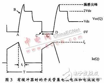
In Figure 1, when Q begins to turn off, its current begins to drop, and the transformer leakage inductance prevents this current from decreasing. A portion of the current will continue through the switch that will be turned off, and another portion will pass through the RC snubber circuit and charge capacitor C. The magnitude of resistor R is related to the charge current. A portion of Ic flows into capacitor C, which slows the rise in collector voltage. By selecting a sufficiently large C, the overlapping portion of the rising voltage and the falling current of the collector can be reduced, thereby significantly reducing the turn-off loss of the switching transistor, and also suppressing the collector leakage peak voltage. The AC phase in Figure 3 is the switch-off phase and the CD is the switch-on phase. The voltage across capacitor C is zero before the switch is turned off. At the turn-off time (time B), C slows down the rising speed of the collector voltage, but is also charged to 2Vdc (in case of ignoring the leakage inductance spike at that moment). The size of the capacitor C not only affects the rate of rise of the collector voltage, but also determines the energy loss at the resistor R. At the moment of Q turn-off, the voltage on C is 2Vdc, which stores 0.5C (2Vdc) 2 joules. If the energy is all consumed on R, the energy consumed on R during the weekly period is:
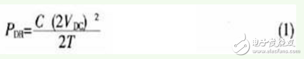
For limiting the collector rising voltage, C should be as large as possible; but from the system efficiency, the larger C, the greater the loss and the lower the efficiency. Therefore, it is necessary to select a suitable C so that it can achieve a certain effect of slowing down the rising voltage of the collector without making the system excessively large and the efficiency is too low.
In Fig. 3, since it is necessary to ensure that there is no voltage across C at the next turn-off start time (time D), C must be discharged during a certain period of time between time B and time D. In fact, the capacitor C can also be discharged through the discharge loop formed by the resistor R through Q and R during the period of the CD. Therefore, after selecting a sufficiently large C, R should cause C to discharge to less than 5% of the charge during the minimum on-time ton, thus:
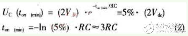
Equation (1) shows that the energy loss on R is proportional to C, so we must choose the appropriate C. Thus, how to choose C becomes the key to design RC snubber circuit. The following is a more practical choice of capacitor C. method.
In fact, when Q begins to turn off, it is assumed that half of the initial peak current Ip flows through C, and the other half still flows through the Q collector that is gradually turned off, while assuming that the leakage inductance in the transformer keeps the total current still Ip. Then, by selecting the appropriate capacitor C, so that the collector collector voltage rises to 2Vdc in time tf (where tf is the time when the collector current drops from the initial value to zero, which can be queried from the switch data sheet), then Have:
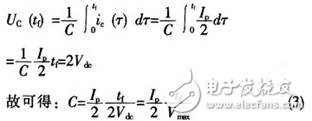
Therefore, the magnitude of the capacitance C can be calculated from the equations (1) and (3). After C is determined, the minimum on-time is known, so that the magnitude of the resistance R can be obtained by the equation (2).
2 main circuit design of forward converter with RC buffer 2.1 Circuit Design Figure 4 shows a forward converter main circuit with an RC snubber circuit. The main circuit parameter is: Np=Nr=43åŒ. Ns=32åŒ, switching frequency f=70 kHz, input voltage range is DC 48~96 V, output is DC 12 V and DC 0.5 A.
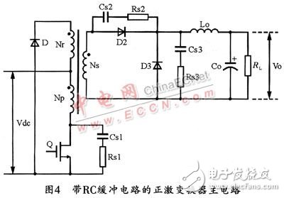
The switch Q is a MOSFET, model IRF830, and its tf is typically 30 ns. Dl, D2, and D3 are fast recovery diodes with a small tf (usually tf = 30 ns). The output power of this design is P0=V0I0=6 W. Assuming that the efficiency of the converter is 80%, the power lost by each RC snubber circuit accounts for 1% of the output power. Take Vdc=48 V here.
2.2 Experimental analysis
The design is analyzed in two cases. The first is that the primary winding has a buffer and the secondary has no buffer. The second is that the primary is unbuffered and the secondary is buffered.
(1) The primary winding is buffered and the secondary is unbuffered
The experiment measures the drain-source voltage across the switch Q. The experiment is divided into the following two cases:
In the first case, RS1 = 1.5 kΩ, CS1 is indeterminate, and the input DC voltage Vdc is 48 V.
The experimental results are as follows: in the case of constant RS1, the larger the CS1 is, although the leakage inductance peak voltage of the switching transistor Q is not significantly reduced, but its drain-source voltage becomes gentle, which indicates the RC buffer in the primary switching tube. In the circuit, CSl should choose a smaller value.
The second case is CSl=33 pF, RS1 is indeterminate, and the input DC voltage Vdc is 48 V. The result is: when CS1 is unchanged, the larger the RS1 is, the larger the leakage inductance peak voltage of the switching transistor Q is (the increase is relatively small).
It can be seen that in the RC snubber circuit, the size of the parameter R has a great influence on reducing the leakage inductance peak. When a suitable C is selected while satisfying equation (2), R should select a relatively small value.
(2) The secondary winding is buffered and the primary is unbuffered.
In this experiment, the cathode of D2 and D3 is used as a common terminal to measure the terminal voltage of the fast recovery diode. As a result, when R is constant, the larger the C, the smaller the leakage inductance peak at both ends of the diode. At the same time, theoretically, if C is infinite, there is no leakage inductance spike in the voltage across the diode. In practice, it is only necessary to make the leakage peak voltage of the voltage across the diode within 30% of the peak value of its terminal voltage, so that the cost is not too high.
2.3 Determination of design parameters
It can be seen from the experimental analysis that in the RC snubber circuit of the secondary fast recovery diode, when the capacitor C of an appropriate size is selected, the resistance R should be selected as small as possible in the case of satisfying the formula (2). Finally, after actual debugging, the RC snubber circuit parameters selected by this design are:
Primary: RS1=200, CSl=100 pF
Secondary: RS2=RS3=5l, CS2=CS3=1000 pF
Although the C value in the RC snubber circuit of the primary switching tube of this design is selected to be slightly larger than the calculated value, the loss is not large, so it is still acceptable. Relative to the primary, the C value in the RC snubber circuit of the secondary fast recovery diode is chosen to be much larger than the calculated value, and the loss of the system must be increased. However, the RC snubber circuit connected in parallel across the fast recovery diode is mainly to improve the system output performance, so choosing a relatively large C value will reduce the overall efficiency of the system, but the leakage inductance peak at both ends of the diode is much reduced, and The ripple of the output voltage can also meet the specified requirements.
According to the formula given above, a suitable RC snubber circuit can be selected very well and conveniently. However, in engineering applications, the actual parameters should be obtained according to the performance indicators of the system design. Sometimes, in order to achieve system performance indicators, it is necessary to sacrifice certain efficiency. In short, when designing RC snubber circuit parameters, we must consider the system performance and efficiency, and finally choose the appropriate RC parameters.
Escalator Lift,Lift Elevator Escalator,Escalator Traction Machine,Indoor Automatic Travelator
XI'AN TYPICAL ELEVATOR CO., LTD , https://www.chinaxiantypical.com