Analog voltages and current references are widely included in analog circuits. In circuits such as digital-to-analog converters and analog-to-digital converters, the accuracy of the reference voltage directly determines the performance of these circuits. This benchmark should have little to do with power and process parameters, but the relationship to temperature is deterministic. In most applications, the required temperature relationship is usually divided into absolute temperature (PTAT) and temperature independent.
In recent years, research has pointed out that when the leakage current remains unchanged, the gate-source voltage of the transistor operating in the weak inversion region decreases approximately linearly within a certain range as the temperature increases. Based on this characteristic, the base-emitter junction employed by the bandgap reference can be replaced by a transistor operating in the weak inversion region to produce a reference source with a low temperature coefficient. The reference source using this design principle is mentioned in the literature, and the amplifier is realized by a low threshold voltage NMOS transistor of 0.13 μm process and a substrate-adjusted PMOS transistor. The reference source circuit used in this paper uses the core circuit principle of the traditional bandgap reference source to compensate the PTAT current dynamic feedback through the saturated MOS equivalent resistance, which basically achieves the stability requirement of the reference source.
1 Basic principles of bandgap referenceThe bandgap reference can have a temperature coefficient of 10 ppm/°C over a temperature range of 0 to 70 °C. The voltage is VBE from a PN junction diode having a temperature coefficient of -2.2 mV/°C at room temperature. At the same time, a thermal voltage VT (VT=kT/q) is generated, which is proportional to the absolute temperature (PTAT). The temperature coefficient at room temperature is 0.085 mV/°C, and the output voltage is:

Equation (1) is used to derive the temperature, and the temperature coefficient of VBE and VT is used to determine the K value that is theoretically independent of temperature. In order to achieve the desired performance, a more detailed analysis of the relationship between VBE and temperature is necessary. The bandgap reference is a weighted addition of the voltage of the negative temperature coefficient to the voltage of the positive temperature coefficient to counteract the effect of temperature on the output voltage.
1.1 Generation of Negative Temperature Coefficient Voltage The base-emitter voltage of a bipolar transistor has a negative temperature coefficient, or the forward voltage of a PN junction diode has a negative temperature coefficient. The relationship between temperature and temperature can be obtained from the literature:
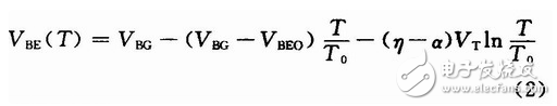
Where: η is the amount associated with the triode structure and has a value of approximately 4; α is an amount related to the current flowing through the triode, and α is 1 when the PTAT current flows through the triode, when the current is unrelated to temperature O is O through the transistor; T0 is the reference temperature; VBG is the bandgap voltage of silicon. It can be seen from equation (1) that VBE is a voltage having a negative temperature coefficient.
1.2 Generation of positive temperature coefficient voltages Two transistors operate at different current densities, and their base-emitter voltages are proportional to the absolute temperature. If two identical transistors (IS1=IS2), the biased collector currents are nI0 and I0, respectively, and their base current is ignored, then:
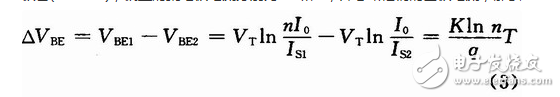
Where: ΔVBE exhibits a positive temperature coefficient, and this temperature coefficient is a constant independent of temperature.
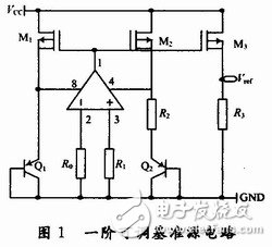
1.3 First-order temperature-compensated bandgap reference source The voltages of the positive and negative temperature coefficients are weighted and added to obtain an approximate temperature-independent reference voltage. A common first-order adjustable reference source circuit is shown in Figure 1.
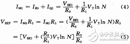
Where: N is the ratio of the emitter junction area of ​​Q2 and Q1, the first term in equation (4) has a negative temperature coefficient, the second term has a positive and negative temperature coefficient, and the ratio of R0 to R1 and the value of N are reasonably designed. , you can get the first-order reference voltage of zero temperature coefficient at a certain temperature. In the square brackets in equation (5), the first-order temperature-independent reference voltage of about 1.25 V is used. By adjusting the ratio of R2/R0, different reference voltages can be obtained.
Figure 2 is the overall circuit diagram of the reference source designed in this paper, including the bandgap core circuit, feedback compensation circuit and startup circuit. The virtual frame a is a band gap core circuit, the virtual frame b is a bias and feedback compensation circuit, and the virtual frame c is a reference source startup circuit.
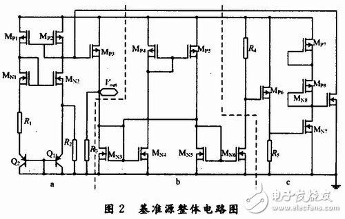
2.1 Bandgap core circuit In Fig. 2, a circuit composed of Mp1 to Mp3, MN1, MN2, R1, R2 and Q1, Q2 constitutes a bandgap core circuit. The bias current of the input transistor is provided by the PMOS current source, which reduces the gm of the load device by reducing its current, rather than reducing its aspect ratio, thereby increasing its differential amplification gain. Among them, Mp1, Mp2, MN1, and MN2 all work in saturation state, and Mp1 and Mp2 duplicate Iout, thus determining IREF. In essence, IREF is "bootstrapped" to Iout. Select a certain MOS tube size. If the substrate trench length modulation effect is ignored, then Iout=KIREF, because each diode-connected device is driven by a current source, so IREF and Iout are independent of VDD. The road always maintains these two current values. Bipolar transistors Q1 and Q2 operate at different current densities, and their base-to-emitter voltage differences are proportional to absolute temperature. A power-independent bias circuit is combined with a bipolar transistor to obtain a bandgap core circuit.
This product response time is shorter than resistive tonch screen's with a good touch.It is widely used to Phone,Tablet,E-book,gaming device by hands holding,Touch Monitor,GPS,All-In-One and so on.GreenTouch projected capacitive touch technology is with fast and sensitive response, the design with frame (without frame is optional) makes it looks professional and generous. The model is designed for high-intensity and high-frequency business environments.
Product show:


Capacitive Touch Screen Panel,Android Touch Screen,Portable Touch Screen,Pcap Touch Screen,POS Terminal Touch Screen,Mini Capacitive Touch Screen
ShenZhen GreenTouch Technology Co.,Ltd , https://www.bbstouch.com