Direct Digital Synthesizer (DDS) technology is a new frequency synthesis principle that directly synthesizes the required waveform based on the concept of phase. It is a signal synthesis technique that converts a series of digital signals into analog signals through DAC. . It has the advantages of fast frequency switching, easy to improve frequency resolution, low hardware requirements, programmable full digitalization for single chip integration, low cost, improved reliability and easy production. At present, major chip manufacturers have successively introduced high-performance and multi-function DDS chips, the internal digital signal jitter is small, and the quality of the output signal is high. However, in some cases, since the control mode of the dedicated DDS chip is fixed, the requirements of the system and the frequency control are very different from those of the system. The interface of the digital controller is inconvenient, it is difficult to meet the complex requirements, and the processing speed is required. Higher, which also limits the further increase in frequency, while the microprocessor's processing tasks are more arduous. FPGA is widely used in electronic product design because of its high reliability, low power consumption and strong confidentiality.
According to the actual needs, this paper designs a three-phase sinusoidal DDS circuit that meets specific needs. It is proved by experiments that the synthesis of DDS by FPGA is a better solution, which has good practicability and flexibility.
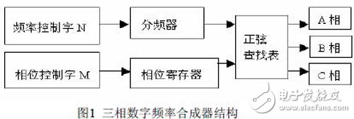
2. Sinusoidal direct digital frequency synthesizer design principleThe synthesizer controls the frequency and phase of the output sine wave by the frequency control word N and the phase control word M, respectively. The phase accumulator is the key control part of the synthesizer. By controlling the speed of the frequency control word N and the phase control word M, the sine wave type of the corresponding frequency and the phase of any lead and lag is obtained, even the cosine wave type. The actual matching of the phase control word M with the frequency control word N is obtained by looking up the sine table address. Each address is actually mapped to each phase point in the range 0-360 in the sine table. The look-up table maps the input address information to the corresponding amplitude to obtain a complete sinusoidal signal. At the same time, through the LPF (low-pass filter) through the digital-to-analog converter DAC, a pure spectrum sine wave can be obtained. The schematic diagram is shown in Figure 1:

In the design of the traditional sinusoidal ROM table, all discrete signals from 0 to 2Ï€ are usually stored in the chip [5]. Although this method is relatively simple to implement, it also wastes a lot of resources of the chip.
Considering that the sine wave signal is evenly symmetric with respect to the straight line X=π from 0 to π and π to 2π, the data in the ROM table can be reduced to half. In the left half cycle, the waveform is oddly symmetric about the line X=π/2, and the sine function ROM table can be further reduced by half. In this way, the data of the ROM table can be reduced to 1/4 of the original, which can greatly reduce the logic resources occupied by the sinusoidal ROM table inside the chip. That is, through the first quarter cycle of a sinusoidal waveform table, the entire periodic waveform of the sinusoid can be transformed, and the cycle resources of nearly 3/4 are reduced to optimize the system, and the effect is very significant.
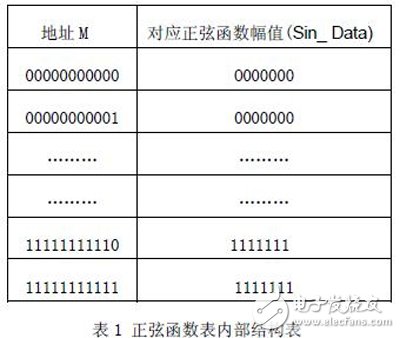
According to the above ideas, the discrete values ​​of the calculated sinusoidal functions are stored in the ROM area of ​​the chip in the order of the corresponding addresses in advance using Equation-1. In the design of this paper, the above idea is adopted, which has a total of 8192 discrete points in a sinusoidal period from 0 to 2π, reduced to 0 to π∕2, a total of 2048 discrete points, wherein the phase resolution is 0.044o. Let N be the address line of the sinusoidal discrete value, and the calculation of the discrete point is calculated according to the formula-1.
Sin_ Data=127&TImes;sin(Ï€/2n) where n is in the range [0,2047] ---- Formula-1 where the internal structure of the sine table is as shown in Table 1:

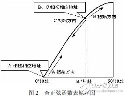
Since a sinusoidal table is used in the design, the need to generate a three-phase sinusoidal signal becomes a difficult and critical point in the logic design. In the traditional design, three sine function tables need to be stored inside the FPGA, which wastes the logic resources of the chip. Therefore, the three-phase sinusoidal signal generated in this paper utilizes the three-phase time-sharing principle design. In the design, three reversible counters are used, which are simultaneously counted under the action of the clock signal, and the count value is used as the address of the three-phase sinusoidal signal in the ROM table. Since the generated three-phase sinusoidal signals are different from each other in the initial phase, the look-up direction of the three reversible counters differs for the three phases A, B, and C under the action of the reversible counter. The principle of the sine function table is shown in Figure 2:

For example, in the design, three three-phase sinusoidal signals with zero initial phase and 120o phase difference are generated. As shown in Figure 2, Phase A begins to accumulate from the address 0° of the sine function table. When the address is read at 90°, it is subtracted from the address 90° to the address 0°, which is reversible in phase A. Under the control of the counter, a unidirectional half-wave sinusoidal signal with a period of π can be obtained; the C phase begins to decrement from the address 60° of the sine function table, and reads from the address 0° and then increments from the address 0°. Read at address 90°, then decrement from address 90° to address 0, so that under the control of phase C reversible counter, one-way half-wave sine with period π and initial phase lag A phase 60° can be obtained. Signal; the same phase B starts from the address 60o of the sine function table, and under the control of the B-phase reversible counter, a one-way half-wave sinusoid with a period of π and an initial phase lag of C phase of 60° can be obtained. Thus, through a sine function table of π/2 cycles, it is possible to emit three unidirectional half-wave sinusoidal signals with a phase difference of 60° and a period of π.
Transparent Led Film Screen P10
With dozens of professional R&D engineers with more than 20 years of experience in the PCB soft film industry as the core, the development of new products is ensured; with dozens of engineers with excellent quality and craftsmanship as the backbone, the product process and quality are ensured. Since its establishment, the business department has followed the business philosophy of "market-oriented, quality-focused, cost-based, and innovation-driven", and the line of self-developed characteristic products. barrier.
Transparent Led Film Screen P10,Led Display Screen P10,Led Display Module Screen P10,Curtain Led Display Transparent Screen
Guangdong Rayee Optoelectronic Technology Co.,Ltd. , https://www.rayeeled.com