The TL494 is a fixed frequency pulse width modulation circuit that includes all the functions required for switching power supply control. It is widely used in bridge single-ended forward double-tube, half-, full-bridge switching power supplies.
1, TL494 internal structure
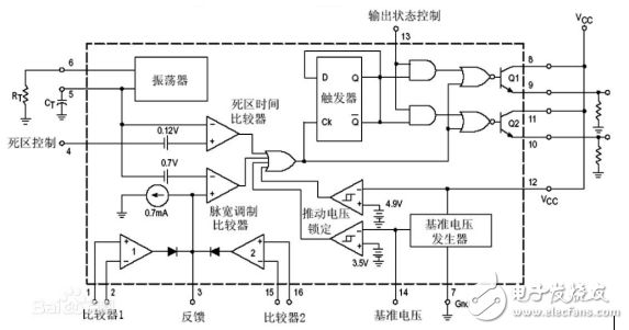
2, the main features
1. Integrated pulse width modulation circuit.
2. The chip has a built-in linear sawtooth oscillator with only two external oscillating components (one resistor and one capacitor).
3. Built-in error amplifier.
4, built-in 5V reference voltage source.
5, can adjust the dead time.
6, built-in power transistor can provide 500mA drive capability.
7, push or pull two output methods.
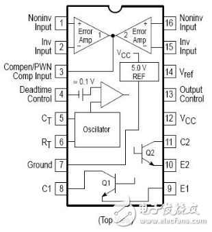
3, pin diagram
1, application one
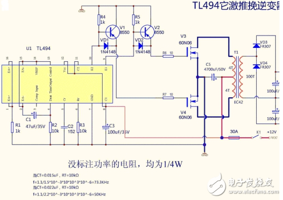
This is the simplest application: the function of two error amplifiers is masked, but the slow-start and dead-band functions are retained. The general application is the most efficient and very stable.
1: According to the manual requirements, the two error amplifiers are shielded. The positive input of the error amplifier is required to be grounded (the 1 pin and the 16 pin are grounded through the 1K resistor), and the negative terminal of the error amplifier is required to be connected to the high potential (2 feet and 15 feet). It is connected to the 14V 5V reference terminal). Note that the 14-pin of the TL494 is a precision regulated power supply with a 5V output. Many applications are sampled from this reference.
In this way, the TL494's 1 pin 2 pin 15 pin 16 pin plus 3 pin (3 pin is the output summary terminal of the two error amplifiers, because the two error amplifiers are shielded, the 3 pin is not considered), the function is not used. It is up.
2: The 4 pin of TL494 is the dead zone control terminal. If the voltage input is 0-4V, the duty cycle can be from maximum to closed (45%-0%). If the 4 pin is directly grounded, the duty cycle is the largest (but Rest assured that the manufacturer has already made a suitable dead zone circuit inside the integrated circuit, 4 feet is directly grounded and there is a dead zone). In the above picture, the 4 pin is used to connect the middle of C1 and R1. The positive pole of the capacitor is connected to the 5V reference potential of the 14 pin, and the capacitor is charged through R1. After the boot, the 4 pin starts to be the potential of 5V until the capacitor is fully charged. 0V (well to complete the duty cycle from 0% to the maximum) The length of the entire slow start is determined by the time constant of C1 and R1 (increasing the resistance or the slow start time of the capacitor becomes longer and vice versa).
3:5 feet and 6 feet are the oscillating frequency. The formula is F=1.1/(R*C). Note that the whole frequency is calculated as the frequency of single-ended applications. If the push-pull application is used, it should be divided by two. Here, the TL494 single-ended application and push-pull application are also mentioned: the 13-pin of the TL494 determines the working mode, and the 13-pin grounding is a single-ended application. If the 14-pin 5V output is connected to the push-pull application. The figure above is the 14-pin push-pull application.
4: 7 feet of TL494 is the power ground, 12 feet are the positive power input terminal 7-40V.
5: TL494 8 feet, 9 feet, 10 feet, 11 feet is the internal triode output pin, because the output current of TL494 is relatively large, if the drive field tube is directly added to the external release tube, it can drive the field tube with relatively large current. So, do a few hundred to kilowatts of power as shown above.
So the simplest application circuit of the TL494 is finished, and only a few components are used in this circuit. But the main features are already covered. Tomorrow, the application of the two error amplifiers of the TL494 will enable the TL494 to perform current limiting, voltage regulation and anti-reverse functions.
2, application two
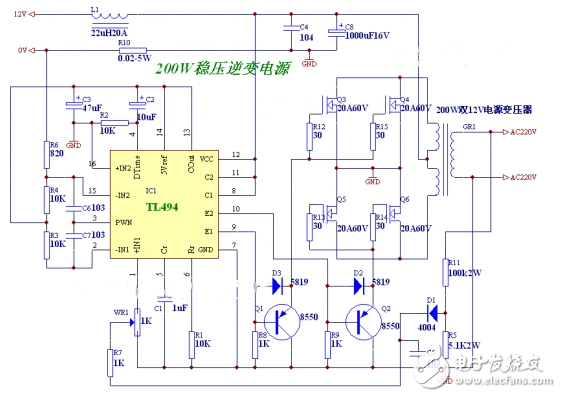
This is a drawing with voltage regulation and current limit, but the application of two error amplifiers is added to the first picture (one for current limiting protection and one for voltage regulation). The two error amplifiers of TL494 allow independent use. However, when using it independently, connect the RC network with the 3 pin of tl494. The c6 and c7 in the above figure play this role.
1: The implementation of the regulation function in the above figure is implemented using pins 1 and 2 of one of the error amplifiers (two error amplifiers can be used interchangeably). Because the 2 pin of the error amplifier is connected to the 14 pin (5V reference voltage terminal) of the TL494 through R3, then the potential of the 2 pin is fixed at 5V, then the potential of the 1 pin must also be stable at 5V. In the above figure, WR1 is based on the need to set the high-voltage output voltage. After the resistor is divided, the voltage is divided and the voltage of the TL494 is maintained at 5V. When the output voltage changes, the potential of the 1 pin of the TL494 will change. The slight change of the potential of the 1 pin causes the error amplifier to control the PWM to automatically adjust the pulse width, and pulls the 1 leg of the TL494 back to 5V in the linear range (that is, the high voltage). Go back to the originally set voltage), so that the voltage regulation requirements are completed.
2: Implementation of the current limiting protection function. In the above figure, the reference voltage is divided by R4 and R6 so that the potential of pin 15 is at (5V*R6)/R4=0.4v, but the other error amplifier is grounded by pin 16. This error amplifier does not function when the approved current is operating. Only when the current of the sampling resistor R10 in the above figure reaches 20A, the potential of the left end of R10 becomes 20A*0.02 ohm=-0.4V with respect to the ground potential. At this time, the potential of pin 15 of TL494 rises to the same potential as that of 16 pin (simultaneous change) The 0 volt error amplifier starts to work. If the current on R10 continues to increase, the duty cycle is reduced by PWM until the output is completely turned off. The normal operating conditions must maintain the potential of 15 feet greater than 0 volts.
The two error amplifiers respectively perform overcurrent and voltage regulation functions to ensure the safe and stable state of the circuit.
You can set the required high voltage and set protection current by adjusting the voltage divider resistors of R3, R4, R6, R10, and TL494 according to the components at hand. (You only need to calculate the above two formulas.) . In addition, the error end of the TL494 has very high impedance and sensitivity (as long as the error terminal input differs by a few MVs, the pulse width can be changed from 0% to 45%), and the resistance of the error input can be selected in a wide range.
Then talk about the replacement of the sampling resistor R10, this resistance is more difficult to find (although the battery car motor controller basically has such a resistance, the diameter of 1.5MM is about 15MM, the resistance is about 0.01 ohm). It is a very important part to prevent the reverse connection of power in the field circuit driven power circuit. The current field tube is small as long as it has a low withstand voltage. This is a screenshot under the Internet, the design is more clever:
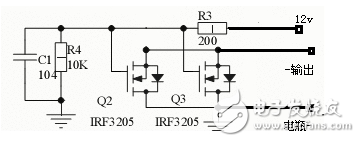
R3 provides the turn-on voltage of the field tube, and R4 and C1 act as current buffers. There are a lot of introductions on the Internet. If the battery input voltage is reversed, there will be almost no current. If the access is correct, a resistor equivalent to a small internal resistance is connected in series. The internal resistance is determined by the selected field tube. For example, the IRF3025 is 0.008 ohms and two parallels are equivalent to a 0.004 ohm resistor. Replacing the resistor R10 with the SD pole of this circuit becomes the circuit that limits the current 100A. Considering that such a large current is not required, the partial voltages of R4 and R6 are taken at 0.2V, (4.7k and 220), which limits the current to about 50A.
When actually doing the second picture, L1 can be canceled, and the positive and negative poles of the battery can be disconnected from the filter capacitor. If there is polarity, the electrolysis will be reversed, but after R10, it must be 10A current and a 2000UF electrolysis requirement. And some high frequency electrolysis (fine high shape electrolysis). In the second figure, as long as the 1 pin is directly grounded, it becomes an open loop application circuit (maximum pulse width operation).
Attach a PCB pattern size 35X35MM:
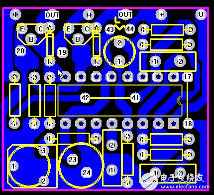
(20 and 19 pads are to be connected)
Next, we will continue to introduce the second-phase high-voltage isolated opto-voltage regulator application, and finally stabilize the high voltage in the hundreds to thousands of volts, the whole machine's no-load current is about 70MA.
Continued: The predecessor "Sisi" sent a picture of SG3525 high-voltage opto-isolated voltage regulator. In fact, this kind of voltage regulation can well meet the PWM voltage regulation requirements. I mentioned earlier that the error end of the TL494 is very sensitive. If all components work in a linear state, the error terminal can control the output high voltage to change from 0V to the highest voltage as long as it detects a few MV to several 10MV changes. A simple application is to use a high-voltage direct series resistor to operate the optocoupler's transmitting end in a suitable linear current range to obtain a suitable feedback voltage at the optocoupler receiving end for comparison.
It is a little troublesome that if the output voltage is not high, it will react relatively quickly with the voltage change, and the resistance of the series optocoupler does not need to consume a lot of power (the general optocoupler must enter the linear state from several MA to several 10MA). ). If the current limit is used at a relatively high output voltage, the current consumption of the current limiting resistor will be relatively large (output 1000v, optocoupler current 3MA is about 3W). There are many ways to solve the optocoupler with the transistor base sampling, or you can use the common TL431 to compare the input sampling drive optocoupler. In this way, the high voltage terminal only needs to input a few UA or tens of UA.
Continued: The following part is a general explanation, PWM circuit voltage regulator is more troublesome. The general principle can be used without it. If you want to use it, you can take the following scheme: The application of TL431 and PC817 is more detailed on the Internet. For particularly high voltage sampling, the input of the TL431 (1 pin) and the power supply of the TL431 cathode (3-pin) optocoupler drive can be separated (additional isolation of 12V windings is simply regulated). The sampling end ground and the 12V winding are connected to the anode of the TL431 (2 feet). The isolation voltage regulation function is completed by feedback of the signal change isolated by the optocoupler to the voltage regulation error terminal of the TL494.
My own voltage feedback processing is not using the error input of the TL494, but using the TL494's 3-pin PWM. Because there is information to find that the 3-step processing of the regulated feedback signal is more stable than the error-end processing.
There are a lot of friends on the circuit will encounter a variety of strange problems, simply put the following attention: First: TL494 power supply filter is very important, two: try to separate the power line. TL494 ground line is also best below Column method trace 8550 ground - TL494 ground (7 feet) - oscillating ground - error so trace. In addition, the shorter the connection of the driving power field tube, the better. There is usually no problem with these details. If there is still a mismatch between the two sides of the push-pull, the transformer is not wound.
Pay attention to the next 84 posts, add a grounding capacitor on the three feet and try the capacity of 0.1U. Having this capacitor seems to greatly improve the waveform.
3, TL494 chip 400W inverter circuit diagram
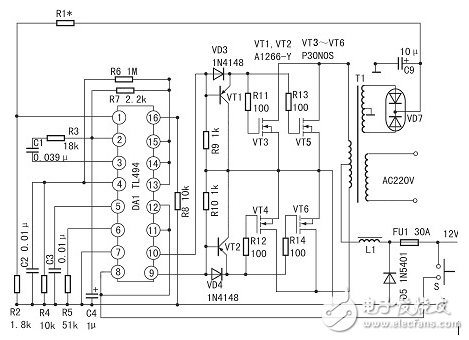
The transformer power is 400VA, and the iron core is made of 45&TImes; 60mm2 silicon steel sheet. The primary winding uses an enameled wire with a diameter of 1.2 mm, two winding around 2 & TImes; 20 inches. The secondary sampling winding is wound with a 0.41 mm enamelled wire and is center tapped. The secondary winding is calculated at 230V and is wound around 400 turns with a 0.8mm enameled wire. The switching tubes VT4 to VT6 can be replaced by any type of N-channel MOS FET tube of 60V/30A. VD7 can be used with 1N400X series of common diodes. The circuit works fine with almost no debugging. When the voltage at the positive terminal of C9 is 12V, R1 can be selected between 3.6 and 4.7kΩ, or adjusted with a 10kΩ potentiometer to make the output voltage rated. If the output power of the inverter is increased to nearly 600W, in order to avoid excessive primary current and increase resistive loss, it is advisable to switch the battery to 24V, and the switch can use a large current MOS FET tube with VDS of 100V. It should be noted that instead of using a single switch with an IDS greater than 50A, the reason is that one is higher in price and the other is too difficult to drive. It is recommended to use 2SK564 with 100V/32A or three 2SK906 parallel applications. At the same time, the cross section of the transformer core should reach 50cm2, calculate the number of turns and the wire diameter according to the calculation method of the ordinary power transformer, or replace the transformer with the waste UPS-600. If you are supplying power to a refrigerator or an electric fan, do not forget to add an LC low-pass filter. A 400W high power regulated inverter circuit composed of TL494. Its excitation conversion part adopts TL494, VT1, VT2, VD3, VD4 constitutes a sink current drive circuit, and drives two two 60V/30A MOS FET switch tubes. If you need to increase the output power, you can use 3 to 4 switch tubes in parallel for each channel, and the circuit will not change.
Starting Relay,Start Preheating Relay,Car Start Relay,Auto Starter Relay
Ningbo Xingchuangzhi Electric Appliance Co.,Ltd. , https://www.xingchuangzhi.com