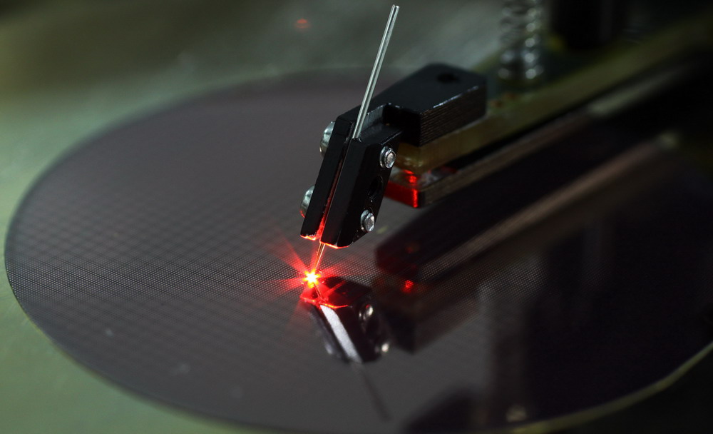
Guide: LED chip, also known as LED light-emitting chip, is the core component of LED light, which is also referred to as PN junction. Its main function is to convert electrical energy into light energy. So what is the size of the LED chip, how the LED chip production process, the following small series will introduce you.
What size does the LED chip have:
High-power LED chips are available in three sizes: 38*38mil, 40*40mil, and 45*45mil. These are just common specifications. Mil is a unit of size, a mil is one thousandth of an inch. 40mil is almost 1 mm. 38mil, 40mil, and 45mil are common size specifications for 1W high power LED chips. In theory, the larger the LED chip, the greater the current and power it can withstand. However, the LED chip material and process are also the main factors affecting the power of the LED chip. For example, some LED chips can withstand 1W to 3W, and other LED chips of the same size can withstand up to 2W.
LED chip manufacturing process:
In general, the LED chip production process is divided into two parts:
First, a gallium nitride (GaN)-based epitaxial wafer was fabricated on a substrate, which was mainly performed in a metal organic chemical vapor deposition epitaxial wafer furnace (MOCVD). After preparing the material source and various high-purity gases required for the fabrication of the GaN-based epitaxial wafer, the epitaxial wafer can be gradually completed according to the requirements of the process. Commonly used substrates are mainly sapphire, silicon carbide and silicon substrates, as well as GaAs, AlN, ZnO and other materials.

MOCVD uses a gas phase reactant (precursor) and a group III organometallic and a group V NH3 to react on the surface of the substrate to deposit the desired product on the surface of the substrate. By controlling the temperature, pressure, reactant concentration, and species ratio, the coating composition and crystal quality are controlled. MOCVD epitaxial furnace is the most commonly used equipment for making LED epitaxial wafers.
Then, the two electrodes of the LED PN junction are processed. Electrode processing is also a key process for making LED chips, including cleaning, evaporation, yellowing, chemical etching, fusion, and grinding. Then, the LED chips are diced, tested, and divided. Select, you can get the required LED chip. If the cleaning of the LED chip is not clean enough, the evaporation system is not normal, and the metal layer (referred to as the electrode after etching) may be peeled off, the appearance of the metal layer is discolored, and the gold bubble is abnormal.
In the evaporation process, it is sometimes necessary to fix the LED chip with a spring clip, so that a pinch is generated (it must be removed in the visual inspection). Huang Guang's work includes baking, photoresist, photographic exposure, development, etc. If the development is not complete and the mask has holes, there will be more metal in the light-emitting area.
In the front-end process of LED chips, various processes such as cleaning, evaporation, yellow light, chemical etching, fusion, grinding, etc. must use tweezers and flower baskets, carriers, etc., so there will be electrode chip scratches.
The IDA system is a new product that Sinco has put on the market in recent years. IDA is an abbreviation for Intelligent Data Collection. The main components of the system are: sensors, multi-channel modules, interface repeaters, terminal boxes, I/R modules, power supplies, personal computers, sensing cables, buses, various lightning protectors, bus power controllers, overvoltages Protector, manual reading adapter and portable reading display, etc. The multi-channel module converts the sensor signal into a digital form and transmits it to the personal computer on site via the IDA bus. The PC will convert the data obtained from the engineering unit and save it to a floppy disk. If necessary, the PC can also analyze and compare the input data to preset alarm limits and issue alarms. Data can be printed, displayed, and can be repeatedly returned from the front PC to the rear PC for many times. The front PC is used for data recording and the rear is used for data analysis, and the data is transmitted by modem or floppy disk. The rear PC is responsible for data archiving, data analysis, drawing and report generation of the database. The Tennessee Engineering Administration (TVA) in the United States adopted IDAS in the monitoring of the Fontena Dam. The system works well and can also be used for the monitoring of landslides and tailings dams.
Efficient Unit Box,Data Acquisition Box,Data Acquisition Unit Box,Integrated Data Acquisition Box
Shenzhen Scodeno Technology Co.,Ltd , https://www.scodenonet.com